A Guide to Multilayer PCB Fabrication Techniques and Best Practices

Key Takeaways
Understanding the intricacies of multilayer PCB fabrication is essential for anyone involved in the electronics industry. You will discover that the efficiency of your designs relies heavily on the pcb manufacturing process, which encompasses a range of techniques from the initial design to final production. As you navigate this field, consider evaluating various pcb manufacturing companies that can provide you with insights into effective layer stack-up considerations and innovative design strategies. Keep in mind that costs may vary and understanding your pcb manufacturing cost can better inform your decisions, allowing you to optimize both performance and budget. Engaging with a reliable pcb manufacturing business will not only help safeguard your design integrity but also enhance reliability through rigorous quality control measures. When exploring these options, it’s important to prioritize companies that adhere to best practices within the industry; this knowledge can lead to a more successful project outcome overall. For further information and resources on PCB services, you might want to visit Andwin PCB.
Introduction to Multilayer PCB Fabrication
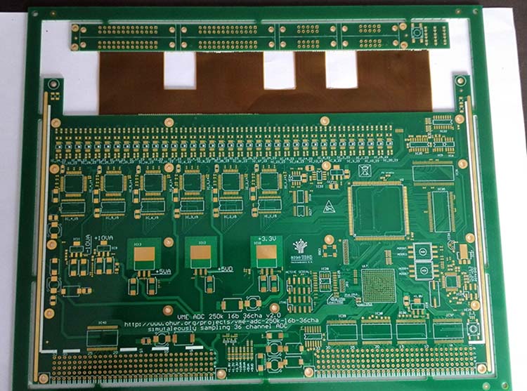
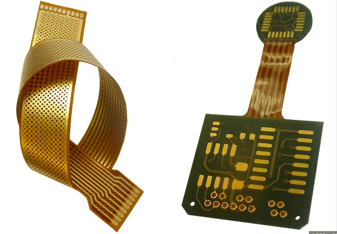
In today’s rapidly evolving electronics landscape, the multilayer PCB fabrication process stands out as a crucial component in the design and production of advanced circuit boards. As you delve into the world of printed circuit boards, understanding this process will enhance your ability to create reliable and high-performance products. Multilayer designs allow you to significantly increase the density and functionality of your circuits by stacking multiple layers of conductive tracks and insulating materials. This approach not only supports complex circuits but also aids in effective signal management, providing a foundation for sophisticated electronic devices.
When engaging with pcb manufacturing processes, it’s important to collaborate with reputable pcb manufacturing companies that emphasize quality and adhere to robust fabrication standards. As you consider various options, keep in mind that the pcb manufacturing cost can vary widely depending on factors such as material choice, layer count, and production efficiency. Engaging with a committed pcb manufacturing business can ensure that your designs are executed flawlessly, which is critical for maintaining signal integrity and overall performance.
“Investing in high-quality multilayer PCB fabrication can dramatically improve both performance and reliability in your electronic applications.”
Understanding the nuances of multilayer PCB fabrication will empower you not only to create innovative designs but also to navigate pricing structures effectively—ultimately enhancing your strategic approach in this competitive field.
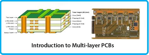
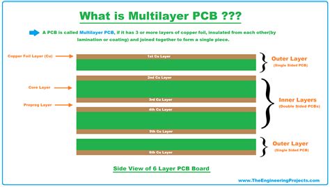
Understanding Layer Stack-Up: Essentials and Guidelines
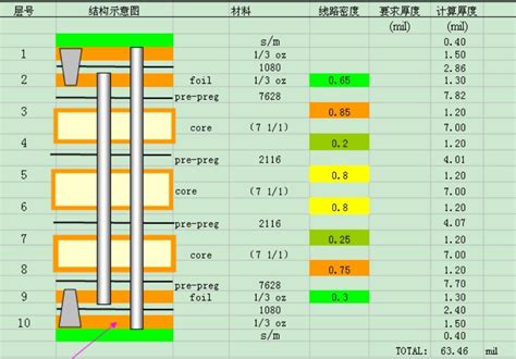
To achieve optimal performance in multilayer PCB fabrication, understanding the layer stack-up is crucial. The stack-up determines the arrangement of layers, which can significantly impact the pcb manufacturing cost and overall functionality of the final product. When designing your multilayer PCB, consider factors such as electromagnetic interference (EMI), signal integrity, and thermal management. A well-thought-out layer arrangement not only enhances performance but also minimizes potential issues during the manufacturing process handled by various pcb manufacturing companies.
You should start by determining the number of layers needed based on your design requirements. For instance, you might need additional layers for power distribution or ground planes to support high-speed signals. Pay close attention to dielectric materials’ thickness between layers and ensure that they complement each other for signal propagation and isolation.
Moreover, incorporating impedance-controlled designs where necessary can help maintain signal integrity across your PCB. This is where you’re likely to witness a significant effect on both the performance and durability of your assembly. Balancing these aspects is essential, particularly when aiming to reduce pcb manufacturing costs while still achieving excellent reliability.
Ultimately, knowing how to effectively manage the layer stack-up can set you apart in a competitive pcb manufacturing business landscape, allowing you to deliver superior products that meet demanding specifications effectively. Prioritize collaboration with skilled engineers who understand these principles as they will guide you through intricate designs that leverage advanced techniques in multilayer PCB fabrication.
Key Techniques for Multilayer PCB Design
When diving into multilayer PCB fabrication, it’s essential to grasp several key techniques that can significantly impact your project’s success. First and foremost, consider the importance of designing an effective layer stack-up. This involves arranging the layers thoughtfully to ensure optimal performance. You want to balance signal integrity and minimize pcb manufacturing costs by selecting materials that offer the best performance-to-cost ratio. Moreover, effective signal routing is critical; using techniques such as differential pair routing can enhance transmission quality.
Another vital consideration is the use of via types. Selecting the appropriate via structures, such as blind, buried, or through vias, can elevate your design’s efficiency and reliability while impacting pcb manufacturing business dynamics. Furthermore, incorporating impedance control measures helps maintain signal consistency across the board. Utilizing coplanar waveguide techniques or adjusting trace widths can facilitate this.
As you design your multilayer PCB, remember to consult with reputable pcb manufacturing companies during the process for insights on their capabilities and best practices in fabrication. Not only can their expertise guide you in making better design choices, but it also ensures that potential issues related to assembly or performance are addressed beforehand.
Ultimately, by leveraging these techniques and maintaining communication with your fabrication partners, you’re not only optimizing for current design requirements but also reducing risks associated with errors in mass production phases of your pcb manufacturing endeavors.
Best Practices for Ensuring Signal Integrity
When it comes to multilayer PCB fabrication, maintaining signal integrity is paramount. You should start by assessing the layer stack-up. Proper layer arrangement is essential for optimizing the performance of your PCB. Utilize ground planes effectively; these not only create return paths for signals but also reduce noise and interference, which are vital for ensuring clean and effective signal transfer. Additionally, pay attention to the trace width and spacing—ensuring they are sized correctly can significantly impact your design’s electrical performance. Incorporating controlled impedance traces can also foster better signal integrity, especially in high-frequency applications.
Moreover, you should consider the effects of via design; using multiple vias can help mitigate impedance discontinuities that might occur at transition points in your PCB layout. Remember that pcb manufacturing techniques employed by various manufacturers may affect this aspect; it is wise to discuss these factors with potential pcb manufacturing companies to select options that best suit your design needs.
Furthermore, keeping track of the pcb manufacturing cost allows you to weigh the benefits of advanced techniques against budget constraints without compromising on quality. Adhering to these best practices not only enhances your design’s functionality but also minimizes potential issues during production and ensures long-term reliability—essentially fortifying your pcb manufacturing business against common pitfalls often experienced in less disciplined approaches. In summary, a meticulous focus on these aspects will go a long way in achieving robust signal integrity in your multilayer PCB designs.
Power Distribution and Grounding Strategies
In multilayer PCBs, effective power distribution and grounding strategies are paramount to ensure optimal performance and reliability. When designing your PCB, you must consider how power is distributed across the layers. One essential practice is to utilize a solid ground plane, which not only minimizes ground bounce but also enhances signal integrity by reducing noise levels. Moreover, keep in mind that the placement of vias can profoundly affect your design. Strategically locating vias ensures that currents can be routed effectively without introducing excessive resistance or inductance, which is critical for high-speed applications.
When working with PCB manufacturing companies, it’s vital to communicate your grounding requirements clearly, as this will influence the PCB manufacturing cost significantly. High-quality PCB manufacturing processes often provide advanced techniques for optimizing power distribution networks, such as using multiple vias for power traces and implementing decoupling capacitors close to critical components. Additionally, establishing a good balance between signal and ground layers helps in managing ground noise effectively, thus maintaining signal clarity. By prioritizing these strategies during the design phase of your PCB manufacturing business, you enhance both the functionality and longevity of your electronic devices.
Common Design Rules for Multilayer PCBs
When engaging in multilayer PCB fabrication, adhering to established design rules is crucial for achieving optimal performance and reliability. One of the primary considerations is the layer stack-up, which should be planned thoughtfully to ensure proper signal integrity and minimize electromagnetic interference. As you define your layer arrangement, consider the use of controlled impedance techniques to maintain consistent signal quality, especially in high-frequency applications.
Moreover, ensure that via diameter is appropriate relative to trace width to avoid manufacturing complications and potential short-circuits, which emphasizes the importance of selecting reputable PCB manufacturing companies that understand your specifications. You must also account for thermal management; adequate spacing between components allows for effective heat dissipation, thereby prolonging the lifespan of your board.
Finally, don’t overlook the impact of PCB manufacturing cost on your design choices. Balancing performance with budget constraints requires a thoughtful approach; purposeful simplification in your layout can help manage costs while still achieving reliability. By following these common design rules, you will enhance the efficiency of your PCB manufacturing business and contribute significantly to the success of your projects.
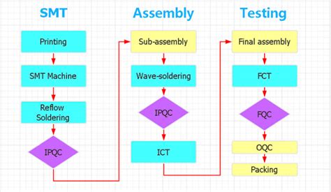
Quality Control Measures in PCB Fabrication
Ensuring the highest quality in PCB manufacturing is crucial for the overall success of your projects. The quality control measures implemented throughout the PCB fabrication process can significantly influence both the reliability and performance of your multilayer designs. To start, you should establish clear standards and criteria for evaluating the performance of each layer during fabrication. This means engaging closely with PCB manufacturing companies that uphold stringent testing protocols, such as Automated Optical Inspection (AOI) and X-ray inspection, which are essential for detecting defects early in the process.
In addition, adopting a robust quality assurance plan that includes regular audits can lead to consistency in production and help reduce overall PCB manufacturing costs. It’s also advisable to ensure that all materials used in your multilayer designs meet required specifications; this can help mitigate issues related to thermal expansion or material degradation over time. Incorporating feedback loops within your design and fabrication process allows you to address any emerging issues quickly while also optimizing for long-term performance.
Investing in advanced testing methodologies, such as signal integrity analysis and thermal cycling tests, can provide insights into how well your multilayer PCB will perform under varying conditions. Remember that a strong focus on quality control not only enhances the reliability of your designs but also reinforces your position within the highly competitive pcb manufacturing business, enabling you to deliver products that meet or exceed customer expectations effectively.
Conclusion: Maximizing Performance and Reliability
In the realm of multilayer PCB fabrication, achieving optimal performance and reliability requires a comprehensive understanding of various techniques and design strategies. By carefully considering factors such as layer stack-up, signal integrity, and grounding strategies, you can significantly enhance the performance of your designs. Additionally, it’s essential to collaborate with reputable PCB manufacturing companies to ensure high-quality results that meet industry standards. The PCB manufacturing cost can vary depending on the complexity of the design and materials used, so exploring different options can lead to cost-effective solutions without compromising quality. Focusing on these aspects not only streamlines the PCB manufacturing business but also elevates your projects to new heights of reliability and efficiency. Ultimately, combining these practices will result in PCBs that perform consistently in demanding environments, ensuring long-term success all while maintaining a clear focus on reliability and efficiency.
Conclusion: Maximizing Performance and Reliability
In the realm of multilayer PCB fabrication, understanding the interplay between various techniques and design rules is crucial for achieving optimal performance and reliability. As you navigate through your PCB manufacturing journey, it’s essential to consider how different pcb manufacturing companies approach layer stack-ups, signal integrity, and power distribution. By implementing best practices tailored to your specific goals, you can effectively minimize costs while enhancing the functionality of your boards. It’s important to be aware of the pcb manufacturing cost implications throughout the design process, as selecting the right materials and technologies can lead to significant savings without compromising quality. Whether you’re running a pcb manufacturing business or helping clients with their design needs, focusing on these foundational elements will ensure that your multilayer PCBs not only meet but exceed performance expectations, paving the way for success in an increasingly competitive field.
FAQs
What are the typical costs involved in pcb manufacturing?
The pcb manufacturing cost can vary greatly depending on several factors, including the complexity of the design, the number of layers, materials used, and additional processes required. It’s crucial to consult with different pcb manufacturing companies to get accurate quotes tailored to your specific requirements.
How can I ensure quality in my multilayer PCB?
To ensure quality in your multilayer PCB, you should adhere to established design rules and guidelines. Engaging experienced pcb manufacturing companies can also help you implement best practices that optimize both performance and reliability.
What should I know about multilayer PCB layer stack-up?
Understanding the layer stack-up is essential for achieving optimal signal integrity and performance. Your design decisions should consider impedance control, ground planes, and the proper arrangement of signals to minimize interference.
Are there specific design rules I should follow?
Yes, following certain design rules is critical when working with multilayer PCBs. This includes defining clearances between traces, choosing appropriate trace widths for current capacity, and ensuring adequate grounding techniques.
How do grounding strategies impact performance?
Effective grounding strategies minimize noise and enhance signal integrity by providing a stable reference point for your signals. Utilizing proper grounding techniques during pcb manufacturing helps in reducing electromagnetic interference (EMI) that can affect device performance.