A Quick Guide on How to Design Full-Color UV Printed PCBs
Introduction
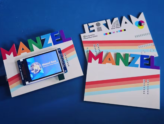
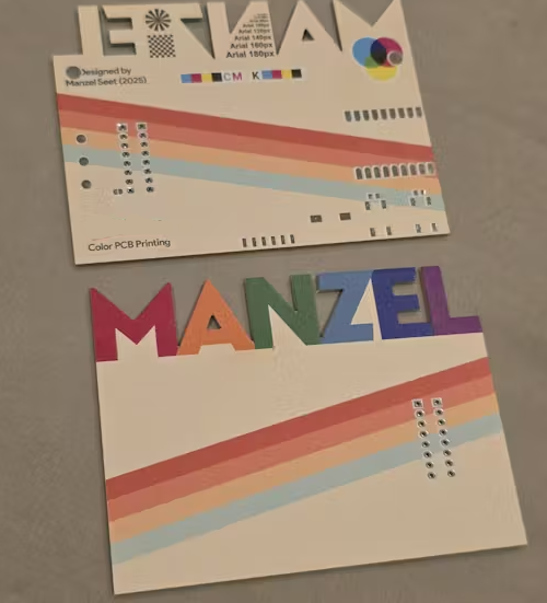
Printed Circuit Boards (PCBs) are the backbone of modern electronics, and their aesthetics are becoming increasingly important for branding, user experience, and functional labeling. Full-color UV printing on PCBs allows for high-resolution graphics, logos, and color-coded components directly on the board surface.
This guide provides a step-by-step approach to designing PCBs with full-color UV printing, covering material selection, design considerations, file preparation, and printing techniques.
1. Understanding Full-Color UV Printing on PCBs
UV printing is a digital printing method that uses ultraviolet light to cure inks instantly. Unlike traditional silkscreen printing, UV printing supports full-color graphics, gradients, and intricate designs with high precision.
Advantages of UV Printing on PCBs:
- High Resolution: Supports fine details (up to 1200 DPI).
- Durability: UV-cured inks are resistant to abrasion, chemicals, and heat.
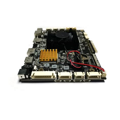
- Versatility: Can print on FR4, flexible PCBs, and metal substrates.
- Fast Turnaround: No need for screens or long drying times.
2. Material Selection for UV-Printed PCBs
The substrate and surface finish impact print quality and adhesion.
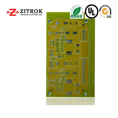
Recommended PCB Materials:
- FR4 (Standard): Works well with UV inks; ensure a smooth surface.
- Flexible PCBs (Polyimide): Requires specialized UV inks for adhesion.
- Metal Core PCBs: Needs a primer layer for better ink bonding.
Surface Finishes:
- OSP (Organic Solderability Preservative): Best for high-resolution printing.
- ENIG (Electroless Nickel Immersion Gold): Good but may require pretreatment.
- HASL (Hot Air Solder Leveling): Less ideal due to uneven surfaces.
3. Design Considerations for UV Printing
A. Artwork Preparation
- Use vector-based design software (Adobe Illustrator, CorelDRAW, or KiCad/Altium for PCB integration).
- Ensure a minimum resolution of 300 DPI for graphics.
- Avoid extremely fine details (<0.1mm) as they may not print clearly.
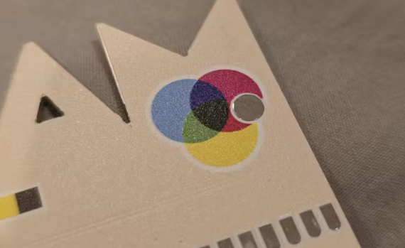
B. Color Management
- Use CMYK color mode for accurate printing.
- Avoid RGB-only designs, as they may shift during conversion.
- For Pantone colors, provide a reference to the PCB manufacturer.
C. Alignment with PCB Layers
- Define a clear registration area (fiducial marks) to align printing with copper layers.
- Keep critical text/logos at least 1mm away from board edges to avoid trimming errors.
D. Ink Limitations
- White ink is often used as a base layer for vibrant colors.
- Transparent inks can create overlays for indicators (e.g., LED zones).
- Avoid large solid ink areas, as they may crack during thermal cycling.
4. File Preparation for Manufacturing
A. Layer Separation
Provide separate files for:
- Copper layers (Gerber files: .GBR)
- Solder mask (.GBR)
- Silkscreen (if needed) (.GBR)
- UV print layer (PDF/AI with CMYK colors)
B. File Formats
- Vector-based: .AI, .PDF, .SVG (for logos/text)
- High-res bitmap: .PNG, .TIFF (300+ DPI)
- Gerber files: Standard .GBR for PCB fabrication
C. Critical Checks Before Submission
- Verify bleed areas (extend graphics slightly beyond cut lines).
- Confirm ink opacity (especially for white underlays).
- Ensure no overlapping with solder mask openings.
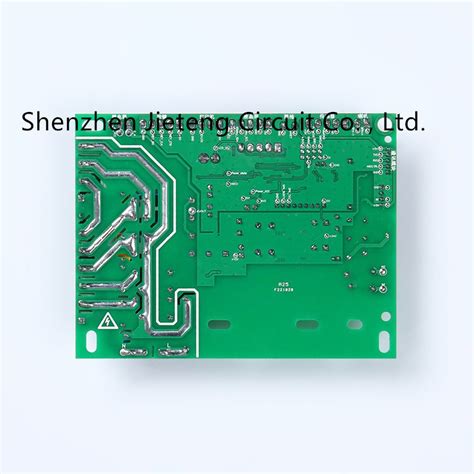
5. UV Printing Process Overview
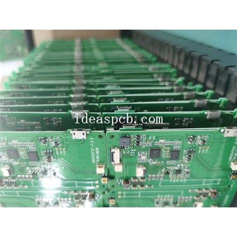
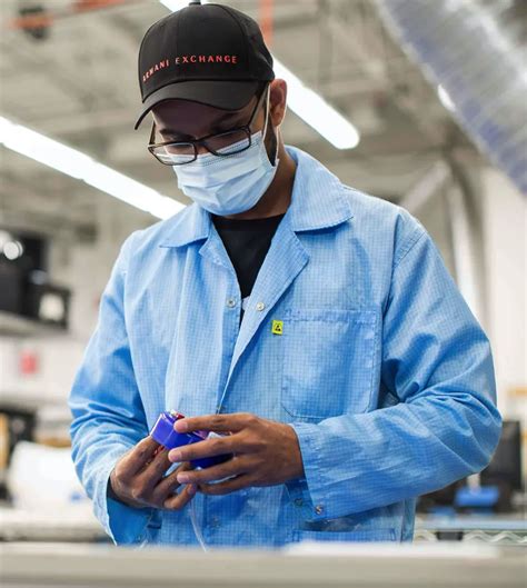
Step 1: PCB Fabrication
- Standard PCB manufacturing (etching, drilling, plating).
- Apply solder mask (if needed) before printing.
Step 2: Surface Treatment (If Required)
- Cleaning (isopropyl alcohol) to remove residues.
- Plasma treatment (for better ink adhesion on difficult surfaces).
Step 3: UV Printing
- Printer applies CMYK (+ white) inks layer by layer.
- UV lamps instantly cure each layer.
Step 4: Final Curing & Protection
- Optional clear UV coating for extra protection.
- Electrical testing and quality inspection.

6. Common Mistakes & How to Avoid Them
| Mistake | Solution |
|---|---|
| Low-resolution artwork | Use vector graphics or 300+ DPI images |
| Misaligned printing | Include fiducial marks in design |
| Ink peeling off | Ensure proper surface treatment (cleaning/plasma) |
| Color inaccuracies | Provide Pantone references or printed samples |
| Over-inking leading to cracks | Use halftones for large color areas |
7. Applications of Full-Color UV Printed PCBs
- Branded Electronics: Custom logos, product labeling.
- Wearables & IoT: Aesthetic designs on consumer devices.
- Educational Kits: Color-coded circuits for learning.
- Military/Aerospace: High-visibility indicators.
Conclusion
Full-color UV PCB printing merges functionality with aesthetics, enabling high-quality graphics directly on circuit boards. By following this guide—optimizing design files, selecting the right materials, and working with a reliable manufacturer—you can achieve professional, durable, and visually striking PCBs.
For best results, collaborate closely with your PCB supplier to ensure compatibility between design intent and manufacturing capabilities.