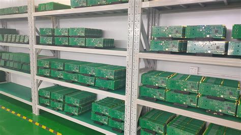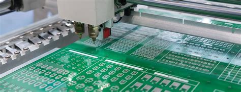
About pcb manufacturing
what is the pcb manufacturing
Generally, the PCB manufacturing process flow chart can be divided into three parts, namely:
● Step 1. PCB manufacturing-preliminary work
● Step 2. PCB manufacturing-production
● Step 3. PCB manufacturing-subsequent measures
Analysis of key process steps in PCB manufacturing.
The manufacturing of printed circuit boards (PCBs) is a complex and delicate process involving multiple key process steps, each of which is critical to ensure the quality and performance of the final product.
- The starting point of PCB manufacturing is the design stage:
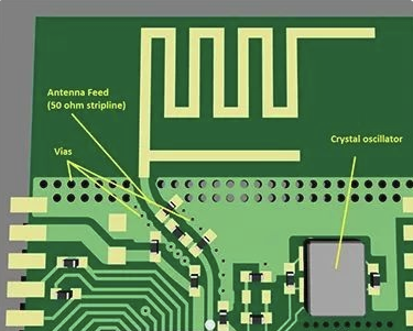
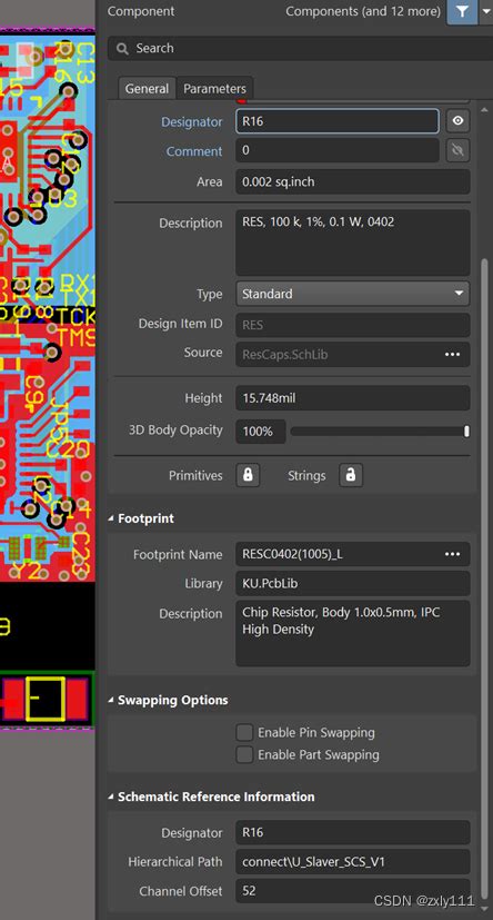
At this stage, engineers use computer-aided design (CAD) software to create detailed layout drawings of the circuit board.
These design drawings not only include the path of the circuit, but also cover the placement and connection of components. After the design is completed, the generated Gerber file will be used to guide subsequent manufacturing steps. - Enter the material preparation stage:
Generally, the substrate of the PCB is a copper clad laminate made of glass fiber reinforced epoxy resin.
The choice of copper clad laminate depends on the application requirements of the circuit board, such as heat resistance, mechanical strength, and electrical properties. After the material is ready, it enters the graphic transfer stage.
At this stage, the circuit pattern in the design drawing is transferred to the copper clad laminate by photolithography.
Specifically, a layer of photosensitive material is coated on the surface of the copper clad laminate, and then the design pattern is accurately transferred to the copper clad laminate through exposure and development. - Enter the etching process:
Etching is to remove the unprotected copper layer, leaving only the copper lines in the design pattern. Common etching methods include chemical etching and plasma etching.
Chemical etching uses acidic or alkaline solutions to dissolve excess copper, while plasma etching uses high-energy plasma to remove excess materials.
After etching is completed, the copper lines on the circuit board are clearly visible, forming the basic framework of the circuit. - It is a drilling and electroplating process:
Drilling is to create through holes on the circuit board to achieve electrical connections between different layers. In modern PCB manufacturing, computer numerical control (CNC) drilling machines are usually used for high-precision drilling.
After drilling is completed, the electroplating process is carried out to plate a layer of copper on the inner wall of the through hole to ensure the reliability of the electrical connection.
The electroplating process not only enhances the conductivity of the through hole, but also improves the mechanical strength of the circuit board. - Enter the pad and surface treatment stage:
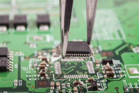
The pad is a metal area for soldering components, usually formed by screen printing or electroplating. Surface treatment is to protect the pad and copper line to prevent oxidation and corrosion.
Common surface treatment methods include hot air leveling (HASL), electroless nickel-gold (ENIG), and organic coating (OSP). - Conduct electrical testing and quality inspection:
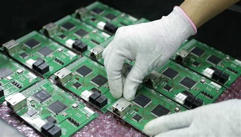
Electrical testing is to ensure that every connection point of the circuit board can work properly, usually using flying probe testing or test fixtures.
Quality inspection includes appearance inspection and functional testing to ensure that the circuit board meets the design requirements and quality standards.
conclusion
the PCB manufacturing process involves multiple key process steps, each of which requires precise control and strict management to ensure the high quality and reliability of the final product.
From design to material preparation, to graphic transfer, etching, drilling, electroplating, pad formation, surface treatment, and final electrical testing and quality inspection, each link is indispensable and together constitutes a complete PCB manufacturing process.
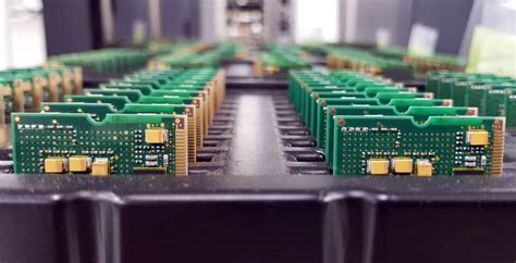
Our PCB manufacturing competences
- Traceability
- Surface-mount technology
- Depaneling
- Through-hole technology
- X-ray analyzing and examining
- In-circuit and functional testing
- Conformal coating
- Box building
PCB manufacturing precautions
- PCB manufacturing precautions
- the details of the design stage should not be ignored.
- the manufacturing process, photolithography and etching processes are key links in determining the quality of PCBs.
- the welding process is also an important link in PCB manufacturing.
In summary, PCB manufacturing is a complex and delicate process, and every link requires strict control and precise operation. Only when material selection, design details, manufacturing process and testing inspection are in place can high-quality and high-reliability PCB products be produced. Therefore, in the PCB manufacturing process, paying attention to every detail and strictly controlling every link are the key to ensuring the quality of the final product.