Adhesiveless flex pcb
Advantages Of Adhesiveless Flex PCB In Modern Electronics
Adhesiveless flex PCBs, or flexible printed circuit boards, have emerged as a pivotal innovation in the realm of modern electronics, offering a multitude of advantages that cater to the ever-evolving demands of contemporary technology. As electronic devices continue to shrink in size while expanding in functionality, the need for more efficient, reliable, and versatile circuit solutions has become paramount. Adhesiveless flex PCBs address these needs by providing a host of benefits that traditional rigid and adhesive-based flexible circuits cannot match.
One of the primary advantages of adhesiveless flex PCBs is their superior flexibility and durability.
Unlike traditional flexible circuits that rely on adhesive layers to bond copper to the substrate, adhesiveless flex PCBs eliminate this layer, resulting in a thinner and more pliable circuit. This increased flexibility allows for more intricate and compact designs, enabling engineers to create devices with complex geometries and tighter spaces. Moreover, the absence of adhesive layers reduces the risk of delamination, thereby enhancing the overall durability and reliability of the circuit, which is crucial for applications subjected to constant bending and flexing.
In addition to their mechanical benefits, adhesiveless flex PCBs offer significant improvements in thermal and electrical performance.
The elimination of adhesive layers reduces thermal resistance, allowing for more efficient heat dissipation. This is particularly advantageous in high-performance applications where heat management is critical to maintaining device functionality and longevity. Furthermore, the direct bonding of copper to the substrate enhances electrical conductivity, resulting in lower signal loss and improved performance. This makes adhesiveless flex PCBs an ideal choice for high-frequency applications, where maintaining signal integrity is of utmost importance.
Another notable advantage of adhesiveless flex PCBs is their contribution to weight and space reduction in electronic devices.
As the demand for portable and lightweight electronics continues to grow, the ability to minimize weight and maximize space becomes increasingly valuable. The thin profile of adhesiveless flex PCBs not only reduces the overall weight of the device but also allows for more efficient use of space, enabling the integration of additional components or features without increasing the device’s size. This is particularly beneficial in industries such as aerospace, automotive, and consumer electronics, where every gram and millimeter count.
Moreover, adhesiveless flex PCBs offer enhanced environmental resistance, making them suitable for a wide range of applications.
The absence of adhesive layers reduces the risk of chemical degradation, ensuring that the circuits can withstand harsh environmental conditions such as extreme temperatures, humidity, and exposure to chemicals. This resilience is essential for applications in demanding environments, such as industrial automation and medical devices, where reliability and longevity are critical.
In conclusion, the advantages of adhesiveless flex PCBs in modern electronics are manifold, encompassing improved flexibility, durability, thermal and electrical performance, weight and space efficiency, and environmental resistance. As technology continues to advance and the demand for more sophisticated electronic devices grows, the role of adhesiveless flex PCBs is set to become increasingly significant. By addressing the limitations of traditional circuit solutions and offering a versatile and reliable alternative, adhesiveless flex PCBs are poised to play a crucial role in shaping the future of electronics, driving innovation and enabling the development of next-generation devices.
Manufacturing Process Of Adhesiveless Flex PCB
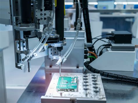
The manufacturing process of adhesiveless flexible printed circuit boards (PCBs) represents a significant advancement in the electronics industry, offering numerous benefits over traditional methods. This innovative approach eliminates the need for adhesive layers, which are typically used to bond copper foil to a flexible substrate. By doing so, it enhances the performance and reliability of the final product, making it an attractive option for various applications, particularly in high-performance and miniaturized electronic devices.
To begin with, the process starts with the selection of a suitable substrate material.
Polyimide is commonly used due to its excellent thermal stability, flexibility, and dielectric properties. The absence of adhesive layers in adhesiveless flex PCBs means that the copper foil is directly laminated onto the substrate. This is achieved through a process known as sputtering or electroplating, where a thin layer of copper is deposited onto the substrate surface. This direct bonding method not only reduces the overall thickness of the PCB but also improves its thermal and electrical conductivity.
Following the deposition of the copper layer, the next step involves the patterning of the circuit.
This is typically done using photolithography, a process that employs light to transfer a geometric pattern from a photomask to a light-sensitive chemical photoresist on the substrate. The photoresist is then developed, revealing the desired circuit pattern. Subsequently, the exposed copper areas are etched away using a chemical solution, leaving behind the intricate circuit design on the substrate.
Once the circuit pattern is established, the next phase involves the application of a protective layer.
This is crucial to safeguard the circuit from environmental factors such as moisture, dust, and mechanical abrasion. A solder mask is often applied, which not only provides protection but also assists in the soldering process by preventing solder bridges between closely spaced pads and traces. Additionally, a surface finish, such as immersion gold or silver, may be applied to enhance the solderability and longevity of the PCB.
The final stages of the manufacturing process include drilling and cutting.
Precision drilling is employed to create vias and holes for component leads, while cutting is used to shape the PCB to its final dimensions. These processes require high precision to ensure that the PCB fits perfectly within its intended application and that all components can be accurately mounted.
Throughout the manufacturing process, rigorous testing and quality control measures are implemented to ensure the reliability and performance of the adhesiveless flex PCB.
Electrical testing is conducted to verify the integrity of the circuit, while mechanical tests assess the flexibility and durability of the board. These quality checks are essential to meet the stringent standards required for modern electronic devices.
In conclusion, the manufacturing process of adhesiveless flex PCBs is a sophisticated and precise operation that offers numerous advantages over traditional methods. By eliminating adhesive layers, these PCBs provide improved performance, reduced thickness, and enhanced reliability, making them ideal for a wide range of applications. As technology continues to advance, the demand for high-performance, miniaturized electronic devices will likely drive further innovations in this field, solidifying the role of adhesiveless flex PCBs in the future of electronics manufacturing.
Applications Of Adhesiveless Flex PCB In Wearable Technology
Adhesiveless flex PCBs, or flexible printed circuit boards, have emerged as a pivotal innovation in the realm of wearable technology. These advanced circuits are characterized by their lack of adhesive layers, which traditionally bond the copper foil to the substrate. This absence of adhesive not only reduces the overall thickness of the circuit but also enhances its flexibility, thermal stability, and electrical performance. As wearable technology continues to evolve, the applications of adhesiveless flex PCBs are becoming increasingly significant, offering numerous advantages that cater to the unique demands of this burgeoning field.
One of the primary applications of adhesiveless flex PCBs in wearable technology is in the development of smartwatches and fitness trackers.
These devices require compact, lightweight, and durable components to ensure user comfort and device longevity. The thin profile and enhanced flexibility of adhesiveless flex PCBs make them ideal for these applications, allowing for seamless integration into the curved and compact designs of modern wearables. Furthermore, the improved thermal management properties of these PCBs help in maintaining optimal device performance, even during prolonged use.
In addition to smartwatches, adhesiveless flex PCBs are also instrumental in the creation of smart clothing.
This innovative category of wearables integrates electronic components directly into fabrics, enabling functionalities such as biometric monitoring, temperature regulation, and even interactive features. The flexibility and durability of adhesiveless flex PCBs allow them to withstand the mechanical stresses associated with clothing, such as bending, stretching, and washing. Consequently, they provide a reliable foundation for embedding electronic circuits into textiles, paving the way for a new era of intelligent apparel.
Moreover, adhesiveless flex PCBs are finding applications in the medical sector, particularly in wearable health monitoring devices.
These devices, which include heart rate monitors, glucose sensors, and other diagnostic tools, require precise and reliable electronic components to ensure accurate data collection and analysis. The superior electrical performance of adhesiveless flex PCBs, combined with their ability to conform to the human body, makes them an excellent choice for medical wearables. By facilitating continuous health monitoring, these devices can significantly enhance patient care and enable proactive health management.
Transitioning from health to lifestyle, adhesiveless flex PCBs are also being utilized in the development of augmented reality (AR) and virtual reality (VR) headsets.
These devices demand high-performance circuits that can handle complex data processing while maintaining a lightweight and comfortable design. The advanced capabilities of adhesiveless flex PCBs meet these requirements, supporting the intricate electronic systems necessary for immersive AR and VR experiences. As these technologies become more integrated into daily life, the role of adhesiveless flex PCBs in enhancing user experience and device functionality will undoubtedly expand.
In conclusion, the applications of adhesiveless flex PCBs in wearable technology are vast and varied, spanning from consumer electronics to medical devices and beyond. Their unique properties, including enhanced flexibility, reduced thickness, and superior thermal and electrical performance, make them indispensable in the design and development of next-generation wearables. As the demand for more sophisticated and versatile wearable technology continues to grow, adhesiveless flex PCBs will play an increasingly critical role in shaping the future of this dynamic industry.

Comparing Adhesiveless Flex PCB To Traditional Flex PCB
In the realm of modern electronics, the evolution of printed circuit boards (PCBs) has been pivotal in advancing technology. Among the various types of PCBs, flexible PCBs have gained significant attention due to their versatility and adaptability in numerous applications. Within this category, adhesiveless flex PCBs have emerged as a noteworthy innovation, offering distinct advantages over traditional flex PCBs. To understand the differences between these two types, it is essential to explore their construction, performance, and applications.
Traditional flex PCBs are typically constructed using a copper foil laminated to a flexible substrate, such as polyimide, with an adhesive layer in between.
This adhesive layer, while serving its purpose of bonding the copper to the substrate, introduces certain limitations. For instance, the adhesive can contribute to increased thickness and reduced flexibility, which may not be ideal for applications requiring tight bending or folding. Moreover, the adhesive layer can be a source of thermal and chemical instability, potentially affecting the long-term reliability of the PCB.
In contrast, adhesiveless flex PCBs eliminate the need for an adhesive layer by directly bonding the copper foil to the flexible substrate through a process known as sputtering or electroplating.
This construction method results in a thinner and more flexible PCB, which can be advantageous in applications where space and weight are critical considerations. The absence of adhesive also enhances the thermal and chemical stability of the PCB, making it more suitable for environments with extreme conditions.
Furthermore, adhesiveless flex PCBs offer improved electrical performance compared to their traditional counterparts.
The direct bonding of copper to the substrate reduces the risk of delamination and ensures better signal integrity, which is crucial in high-frequency applications. Additionally, the absence of an adhesive layer minimizes the dielectric loss, thereby enhancing the overall efficiency of the circuit.
Despite these advantages, it is important to acknowledge that adhesiveless flex PCBs may not be the ideal solution for every application.
The manufacturing process for adhesiveless flex PCBs can be more complex and costly compared to traditional methods, which may not be justifiable for all projects. However, for applications where performance, reliability, and miniaturization are paramount, the benefits of adhesiveless flex PCBs often outweigh the additional costs.
In terms of applications, adhesiveless flex PCBs are particularly well-suited for industries such as aerospace, medical devices, and consumer electronics, where the demand for lightweight, compact, and reliable components is ever-increasing. For instance, in the aerospace industry, the reduced weight and enhanced durability of adhesiveless flex PCBs contribute to improved fuel efficiency and performance. Similarly, in medical devices, the flexibility and reliability of these PCBs enable the development of advanced diagnostic and monitoring equipment.
In conclusion, while both traditional and adhesiveless flex PCBs have their respective merits, the choice between the two ultimately depends on the specific requirements of the application. By understanding the differences in construction, performance, and suitability for various environments, engineers and designers can make informed decisions that align with their project goals. As technology continues to advance, the role of adhesiveless flex PCBs is likely to expand, offering new possibilities for innovation across diverse fields.