Advanced Assembly Circuit Optimization Techniques for Electronics

Key Takeaways
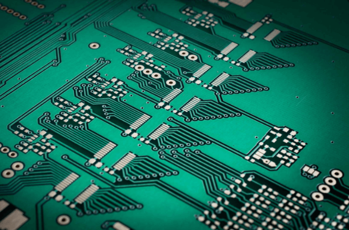
Optimizing PCB assembly processes requires balancing miniaturization demands with thermal and signal integrity considerations. Modern PCBA designs leverage precision component placement to minimize parasitic effects, while advanced routing techniques mitigate electromagnetic interference in high-density layouts. A critical focus lies in thermal dissipation strategies, such as incorporating copper pours or heat sinks, to maintain reliability in compact systems.
Tip: Prioritize iterative prototyping during PCB assembly to identify thermal bottlenecks and signal degradation points early in the design phase.
Key innovations include the use of embedded components and microvia technologies, which reduce footprint without compromising performance. For PCBA workflows, automated optical inspection (AOI) and 3D X-ray analysis ensure alignment accuracy, particularly in multilayer configurations. Additionally, impedance-controlled routing and differential pair optimization preserve signal integrity across high-speed interfaces.
"The interplay between component density and thermal management defines the success of modern PCB assembly."
By integrating simulation tools during the PCBA phase, engineers can preemptively address thermal expansion mismatches and crosstalk. This proactive approach aligns with industry trends toward heterogeneous integration, where mixed-signal layouts demand meticulous planning for both analog and digital domains.
PCB Layout Optimization for Circuit Performance
Optimizing PCB assembly layouts is critical for achieving peak circuit performance in modern electronics. At the core of PCBA design, strategic component placement minimizes parasitic inductance and capacitance while reducing electromagnetic interference (EMI). For instance, grouping analog and digital components separately prevents noise coupling, and positioning high-speed traces away from voltage regulators preserves signal integrity.
Advanced routing techniques further enhance performance. Using PCB assembly design rules, engineers implement differential pair routing for balanced signal transmission and employ via-in-pad technology to reduce inductance in compact layouts. The table below summarizes key optimization strategies:
| Technique | Impact on Performance | Application Example |
|---|---|---|
| Controlled Impedance Routing | Reduces signal reflections | High-frequency RF circuits |
| Thermal Relief Pads | Improves solder joint reliability | Power management ICs |
| Copper Pour Shielding | Mitigates EMI | Mixed-signal systems |
To address thermal challenges in PCBA, designers integrate thermal vias beneath heat-generating components like FPGAs or voltage converters, ensuring efficient heat dissipation. Additionally, optimizing trace widths based on current requirements prevents overheating while maintaining power delivery efficiency. By balancing these factors, engineers achieve layouts that meet both electrical and mechanical demands, particularly in space-constrained devices requiring high reliability.
Thermal Management in High-Density Circuit Assemblies
Effective thermal management is critical in modern PCB assembly designs, particularly as component density increases to meet miniaturization demands. In high-density PCBA configurations, heat accumulation can degrade performance, reduce lifespan, or cause catastrophic failures. Engineers address this by integrating thermally conductive materials, such as metal-core substrates or ceramic-filled laminates, which dissipate heat more efficiently than traditional FR-4 boards.
Strategic placement of thermal vias and copper pours beneath power-hungry components—like processors or voltage regulators—creates low-resistance pathways for heat transfer. Advanced PCB assembly workflows also employ simulation tools to model thermal gradients, enabling preemptive adjustments to component spacing or airflow patterns. For instance, pairing active cooling solutions (e.g., micro-fans or heat sinks) with optimized trace routing ensures even heat distribution without compromising signal integrity.
In high-reliability applications, such as aerospace or medical devices, PCBA designs often incorporate phase-change materials or embedded heat pipes to manage extreme thermal loads. Testing under real-world conditions—including thermal cycling and infrared imaging—validates these strategies, ensuring stability across operational extremes. By balancing material science, layout precision, and predictive modeling, engineers achieve robust thermal performance in even the most densely packed circuits.
Precision Component Placement for Compact Electronics
Effective PCB assembly in compact electronics hinges on meticulous component placement to balance spatial efficiency with functional performance. Miniaturization demands that PCBA engineers prioritize critical components like microcontrollers, sensors, and power modules, ensuring their positions minimize signal interference and optimize thermal pathways. Advanced CAD tools enable precise simulation of electromagnetic compatibility (EMC) and heat distribution, allowing designers to identify optimal layouts before prototyping.
A key consideration is aligning component orientation with high-density interconnect (HDI) substrates to reduce parasitic inductance and capacitance. For instance, placing decoupling capacitors closer to power pins or positioning heat-sensitive ICs away from voltage regulators can significantly enhance reliability. Automated pick-and-place systems achieve micron-level accuracy, vital for maintaining signal integrity in tightly packed designs. Additionally, thermal vias and copper pours are strategically integrated to dissipate heat without compromising spatial constraints.
By harmonizing electrical performance with mechanical stability, PCB assembly teams ensure that compact layouts meet both functional and durability standards. This approach not only supports PCBA scalability but also aligns with emerging trends in wearable tech and IoT devices, where every millimeter impacts usability and efficiency.
Advanced Routing Techniques for Signal Integrity
Achieving optimal signal integrity in PCB assembly requires meticulous attention to routing strategies, particularly in high-speed or mixed-signal designs. Differential pair routing minimizes electromagnetic interference (EMI) by ensuring balanced trace lengths and spacing, while impedance-controlled routing preserves signal quality across transmission lines. For PCBA designs involving dense layouts, techniques like via stitching and ground plane optimization reduce crosstalk and stabilize reference potentials.
Transitioning from component placement to routing, designers must prioritize minimizing path lengths between critical components, such as oscillators or high-speed connectors. Serpentine routing, when applied judiciously, compensates for timing skew without introducing excessive inductance. Additionally, 3D field solvers and simulation tools enable precise analysis of signal reflections and losses before prototyping, reducing iterative fixes in later PCB assembly stages.
In multi-layer boards, strategic use of buried vias and microvias maintains signal integrity while accommodating miniaturization trends. However, thermal management considerations—such as avoiding heat-sensitive traces near power components—must align with routing decisions. By integrating these advanced techniques, PCBA teams can ensure robust performance in applications ranging from IoT devices to aerospace systems, where signal fidelity is non-negotiable.
Miniaturization Trends in Modern Circuit Design
The relentless push toward smaller, more powerful electronic devices has made PCB assembly optimization a cornerstone of modern circuit design. As components shrink to meet nanoscale dimensions, engineers face unprecedented challenges in balancing spatial constraints with electrical performance. Advanced PCBA processes now leverage surface-mount technology (SMT) to place ultra-compact ICs and passive components with micron-level precision, enabling dense layouts without compromising functionality.
A critical driver of miniaturization is the integration of high-density interconnect (HDI) PCBs, which utilize micro-vias and stacked layers to reduce footprint while maintaining signal integrity. These designs demand meticulous PCB assembly workflows, where even minor misalignments can lead to thermal bottlenecks or electromagnetic interference. To address this, automated optical inspection (AOI) systems are increasingly deployed during PCBA stages to validate component placement accuracy in real time.
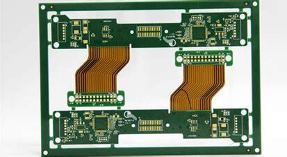
Equally critical is the adoption of flexible and rigid-flex PCBs, which conform to irregular geometries in wearables and IoT devices. This trend necessitates novel routing strategies, such as embedded trace technology, to eliminate bulky connectors. However, shrinking form factors amplify heat dissipation challenges, requiring designers to integrate thermal vias and conductive substrates early in the PCB assembly process. By harmonizing these innovations, modern electronics achieve unprecedented miniaturization without sacrificing reliability or performance.
Ensuring Reliability Through Assembly Optimization
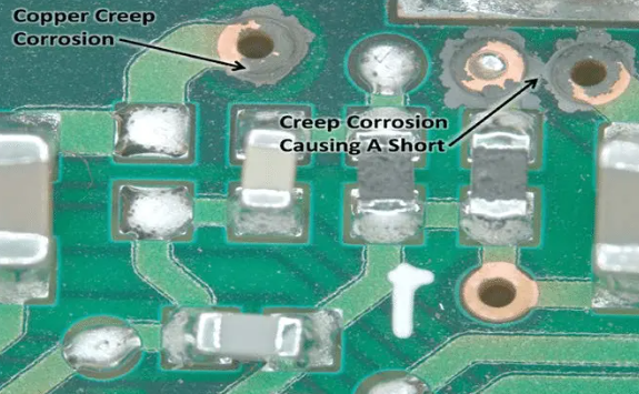
Achieving long-term reliability in modern electronics demands meticulous attention to PCB assembly processes, particularly in high-density designs. Critical factors such as component selection, solder joint integrity, and material compatibility directly influence the durability of PCBA (printed circuit board assembly). By optimizing placement accuracy during PCB assembly, engineers minimize mechanical stress on sensitive components, reducing risks of microfractures or connection failures under thermal cycling.
Advanced PCBA workflows leverage automated optical inspection (AOI) systems to detect microscopic defects in real time, ensuring compliance with stringent quality standards. Additionally, thermal management integration—such as selecting substrates with optimal thermal conductivity—prevents localized overheating, a common cause of premature circuit degradation. For compact systems, strategic routing of power and ground planes enhances electromagnetic compatibility (EMC), mitigating interference that could compromise signal stability.
Transitioning from design to production, reliability-focused PCB assembly prioritizes solder paste formulation and reflow profiling to avoid voids or cold joints. Environmental stressors like humidity and vibration are addressed through conformal coatings or underfill materials, which protect interconnects in harsh operating conditions. By aligning these techniques with rigorous testing protocols, manufacturers ensure that PCBA outputs meet both performance benchmarks and lifecycle expectations for mission-critical applications.
Thermal Dissipation Strategies in PCB Design
Effective thermal management remains critical in modern PCB assembly processes, particularly for high-density PCBA designs where component miniaturization amplifies heat generation. Engineers prioritize thermal vias and copper pours to distribute heat evenly across layers, reducing localized hotspots that compromise reliability. Strategic placement of thermal interface materials (TIMs), such as thermally conductive adhesives or pads, bridges gaps between heat-generating components and heatsinks, enhancing dissipation efficiency.
In multi-layer designs, stackup optimization plays a pivotal role—integrating power and ground planes with thicker copper weights improves heat spreading while maintaining signal integrity. For compact layouts, embedded cooling solutions, including microfluidic channels or passive heat pipes, offer scalable alternatives to traditional heatsinks. Simulation tools like computational fluid dynamics (CFD) enable precise modeling of airflow and thermal gradients, allowing iterative refinements during the PCBA prototyping phase.
Material selection further influences performance: substrates with high glass transition temperatures (Tg) and low coefficient of thermal expansion (CTE) mitigate warping under thermal stress. Combining these strategies ensures robust operation in demanding environments, aligning with broader objectives of PCB assembly optimization for reliability and longevity. Transitioning to signal integrity considerations, these thermal solutions must coexist with routing techniques that minimize electromagnetic interference—a balance achieved through holistic design frameworks.
Signal Integrity Solutions for Complex Layouts
Maintaining signal integrity in densely packed PCB assembly designs requires addressing challenges like impedance mismatches, crosstalk, and electromagnetic interference (EMI). Modern high-speed and multi-layer PCBA layouts demand meticulous planning, starting with controlled-impedance routing to minimize reflections. By leveraging ground planes and shielding traces, engineers can isolate sensitive signals from noise sources, ensuring stable data transmission.
A critical strategy involves optimizing differential pair routing to preserve timing alignment, particularly in high-frequency applications like RF or DDR memory interfaces. Advanced simulation tools, integrated into PCB assembly workflows, enable pre-layout analysis to predict signal degradation and adjust trace geometries proactively. For instance, adjusting trace widths or spacing between adjacent signals reduces capacitive coupling and mitigates crosstalk.
Thermal management also intersects with signal integrity, as temperature fluctuations alter material properties like dielectric constants. Incorporating thermal vias near heat-generating components in PCBA designs helps stabilize operating conditions, indirectly preserving signal quality. Additionally, controlled-depth blind vias and buried vias in complex stackups minimize stub effects, which can distort high-speed signals.
Finally, post-layout validation through time-domain reflectometry (TDR) and eye diagram analysis ensures compliance with performance thresholds. These techniques, combined with adherence to IPC-2152 standards for current-carrying capacity, create robust solutions for balancing miniaturization demands with uncompromised signal fidelity.
Conclusion
The evolution of PCB assembly techniques underscores the critical balance between performance, reliability, and space efficiency in modern electronics. As explored in this article, advancements in PCBA design prioritize thermal dissipation and signal integrity through intelligent component placement, multilayer routing architectures, and material innovations. From high-density layouts to adaptive thermal management systems, engineers now leverage computational modeling and automated precision tools to overcome the challenges of compact electronic systems.
Ultimately, the success of PCB assembly optimization lies in harmonizing miniaturization trends with robust performance metrics. By integrating advanced routing protocols and proactive thermal strategies, PCBA workflows achieve error-free signal transmission while mitigating heat accumulation in confined spaces. These methodologies not only extend product lifespans but also align with sustainability goals by reducing material waste and energy consumption. As the industry progresses, the interplay between design flexibility and manufacturing precision will remain pivotal in shaping next-generation electronic assemblies.
Frequently Asked Questions
How does thermal management impact PCB assembly reliability?
Effective thermal management in PCBA ensures heat dissipation from high-power components, preventing overheating and extending circuit lifespan. Techniques like thermal vias and copper pours optimize heat distribution in compact layouts.
What role does component placement play in signal integrity ?
Precision placement during PCB assembly minimizes signal path lengths and reduces electromagnetic interference. Strategic positioning of sensitive components is critical for maintaining high-frequency performance in dense PCBA designs.
Can advanced routing techniques improve power efficiency in compact systems?
Yes, optimized routing in PCBA reduces resistive losses and voltage drops. Differential pairing and length-matching traces enhance signal stability, while minimizing crosstalk in high-speed circuits.
How do miniaturization trends affect thermal dissipation strategies?
Smaller PCB assembly designs require innovative cooling solutions, such as embedded heat sinks or thermally conductive substrates. Balancing component density with airflow pathways is essential to prevent hotspots.
What quality controls ensure reliability in optimized PCB assemblies ?
Automated optical inspection (AOI) and functional testing verify solder joint integrity and component alignment. Rigorous testing protocols address thermal cycling and vibration resistance in final PCBA validation.
Explore Customized PCB Assembly Solutions
Ready to enhance your circuit performance? Click here to discover tailored PCB assembly services for your advanced electronics projects.