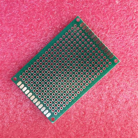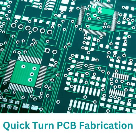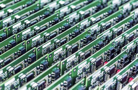
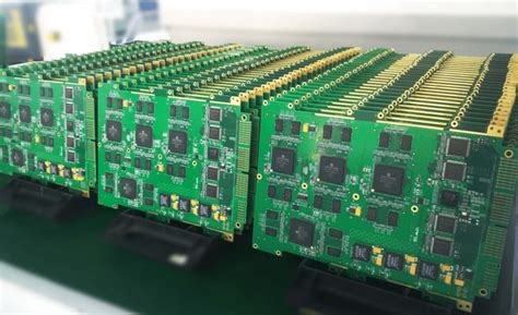
Advanced circuits pcb assembly
Innovations In Surface Mount Technology (SMT) For Advanced circuits pcb Assembly
Surface Mount Technology (SMT) has revolutionized the field of advanced Printed Circuit Board (PCB) assembly, offering significant improvements in efficiency, reliability, and miniaturization. As the demand for more compact and powerful electronic devices continues to grow, innovations in SMT have become crucial in meeting these requirements.
One of the most notable advancements in SMT is the development of smaller and more efficient components.
These components, often referred to as micro-components, allow for higher component density on PCBs, which in turn enables the creation of smaller and more complex electronic devices. This miniaturization is particularly important in industries such as consumer electronics, medical devices, and aerospace, where space and weight are critical factors.
In addition to the miniaturization of components, advancements in soldering techniques have also played a significant role in the evolution of SMT.
Traditional soldering methods, such as wave soldering, have been largely replaced by more precise techniques like reflow soldering. Reflow soldering involves the application of solder paste to the PCB, followed by the placement of components and the application of heat to melt the solder and create strong, reliable connections. This method not only improves the quality of the solder joints but also allows for the use of more delicate and complex components that would be damaged by the higher temperatures and mechanical stresses associated with wave soldering.
Another key innovation in SMT is the development of advanced inspection and testing methods.
Automated Optical Inspection (AOI) and X-ray inspection systems have become essential tools in the PCB assembly process, allowing for the rapid and accurate detection of defects such as solder bridges, component misalignment, and voids in solder joints. These inspection systems not only improve the overall quality and reliability of the assembled PCBs but also help to reduce production costs by identifying and addressing issues early in the manufacturing process.
Furthermore, the integration of advanced materials and processes has also contributed to the advancements in SMT.
For example, the use of high-performance substrates, such as ceramic and flexible materials, has enabled the development of PCBs that can withstand extreme temperatures, mechanical stresses, and harsh environmental conditions. Additionally, the adoption of lead-free solder materials, driven by environmental regulations and industry standards, has led to the development of new solder alloys that offer improved performance and reliability compared to traditional lead-based solders.
The implementation of Industry 4.0 principles in SMT has also brought about significant improvements in the efficiency and flexibility of PCB assembly processes.
The use of advanced robotics, machine learning algorithms, and real-time data analytics has enabled the creation of highly automated and adaptive manufacturing environments. These smart factories can quickly respond to changes in production requirements, optimize resource utilization, and minimize downtime, resulting in increased productivity and reduced costs.
Moreover, the collaboration between industry and academia has played a crucial role in driving innovations in SMT.
Research institutions and universities have been at the forefront of developing new materials, processes, and technologies that have been subsequently adopted by the industry. This collaboration has not only accelerated the pace of innovation but also ensured that the latest advancements are quickly translated into practical applications.
In conclusion, the continuous advancements in Surface Mount Technology have significantly enhanced the capabilities of advanced PCB assembly. Through the development of smaller components, improved soldering techniques, advanced inspection methods, innovative materials, and the integration of Industry 4.0 principles, SMT has enabled the creation of more compact, reliable, and efficient electronic devices. As the demand for advanced electronics continues to grow, ongoing innovations in SMT will remain essential in meeting the evolving needs of various industries.

Challenges And Solutions In High-Density Interconnect (HDI) PCB Assembly
High-Density Interconnect (HDI) PCB assembly represents a significant advancement in the field of electronics, enabling the creation of more compact, efficient, and powerful devices. However, the process of assembling HDI PCBs is fraught with challenges that require innovative solutions to ensure reliability and performance.
One of the primary challenges in HDI PCB assembly is the miniaturization of components.
As devices become smaller, the components used in their construction must also shrink, leading to difficulties in handling and placement. The reduced size of components increases the risk of misalignment and defects during assembly. To address this issue, advanced pick-and-place machines equipped with high-precision vision systems are employed. These machines can accurately position tiny components, ensuring proper alignment and reducing the likelihood of errors.
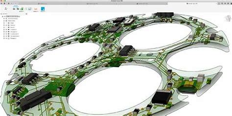
Another significant challenge is the increased complexity of the PCB design.
HDI PCBs often feature multiple layers, microvias, and fine traces, which complicate the manufacturing process. The intricate design requires precise control over the drilling and plating processes to ensure the integrity of the connections. To overcome this, manufacturers utilize laser drilling technology, which offers superior accuracy and consistency compared to traditional mechanical drilling methods. Additionally, advanced plating techniques, such as electroless copper deposition, are employed to create reliable connections between layers.
Thermal management is also a critical concern in HDI PCB assembly.
The high component density and increased power consumption generate significant heat, which can adversely affect the performance and longevity of the device. Effective thermal management solutions, such as the use of thermal vias, heat sinks, and advanced materials with high thermal conductivity, are essential to dissipate heat efficiently. Moreover, thermal simulation software can be used during the design phase to predict and mitigate potential thermal issues.
Signal integrity is another area where HDI PCB assembly faces challenges.
The close proximity of traces and components can lead to signal interference and crosstalk, which can degrade the performance of the device. To address this, designers must carefully consider the layout and routing of traces, employing techniques such as differential signaling and controlled impedance routing. Additionally, the use of advanced materials with low dielectric constants can help minimize signal loss and maintain signal integrity.
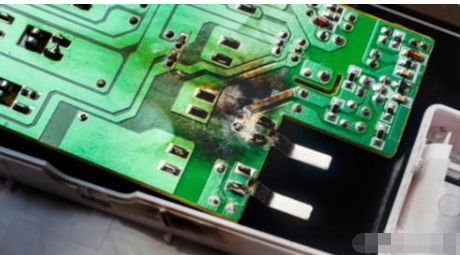
The assembly process itself presents challenges related to soldering and reflow.
The small size of components and fine pitch of pads require precise control over the soldering process to avoid defects such as solder bridges and insufficient solder joints. Advanced soldering techniques, such as laser soldering and selective soldering, offer greater precision and control compared to traditional methods. Furthermore, the use of high-quality solder pastes and fluxes can improve the reliability of solder joints.
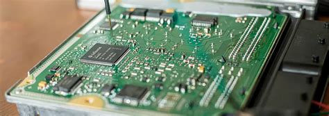
Quality control and testing are crucial in ensuring the reliability of HDI PCBs.
The complexity and miniaturization of these boards make traditional inspection methods less effective. Advanced inspection techniques, such as automated optical inspection (AOI) and X-ray inspection, are employed to detect defects that may not be visible to the naked eye. Additionally, functional testing and in-circuit testing (ICT) are used to verify the performance of the assembled PCB.
In conclusion, while HDI PCB assembly presents numerous challenges, advancements in technology and innovative solutions have enabled manufacturers to overcome these obstacles. By employing high-precision equipment, advanced materials, and sophisticated design techniques, it is possible to produce reliable and high-performance HDI PCBs that meet the demands of modern electronic devices. As technology continues to evolve, further advancements in HDI PCB assembly are expected, paving the way for even more compact and powerful electronic devices.
The Role Of Automated Optical Inspection (AOI) In Ensuring PCB Quality
In the realm of advanced circuits PCB assembly, ensuring the highest quality of printed circuit boards (PCBs) is paramount. One of the most critical technologies employed to achieve this objective is Automated Optical Inspection (AOI). AOI systems play a pivotal role in the detection and correction of defects during the PCB manufacturing process, thereby enhancing the overall reliability and performance of electronic devices.
Automated Optical Inspection utilizes high-resolution cameras and sophisticated algorithms to scrutinize PCBs for a variety of potential defects.
These defects can range from soldering issues, such as insufficient or excessive solder, to component misalignments and missing components. By capturing detailed images of the PCB and comparing them to a predefined set of standards, AOI systems can identify anomalies with remarkable precision. This capability is particularly crucial in advanced circuits, where even minor defects can lead to significant performance issues or complete device failure.
Transitioning from traditional manual inspection methods to AOI offers several advantages.
Firstly, AOI systems provide a level of consistency and accuracy that is difficult to achieve through human inspection alone. Human inspectors, despite their expertise, are prone to fatigue and subjective judgment, which can result in overlooked defects. In contrast, AOI systems operate with unwavering consistency, ensuring that each PCB is inspected to the same rigorous standards. This consistency is essential in maintaining the high quality required for advanced circuits.
Moreover, AOI systems significantly enhance the efficiency of the inspection process.
Manual inspection is time-consuming and labor-intensive, often leading to bottlenecks in the production line. AOI systems, however, can inspect PCBs at a much faster rate, thereby streamlining the manufacturing process. This increased efficiency not only reduces production costs but also accelerates time-to-market, giving manufacturers a competitive edge in the fast-paced electronics industry.
In addition to defect detection, AOI systems also play a crucial role in process optimization.
By providing detailed feedback on the types and frequencies of defects, AOI systems enable manufacturers to identify and address underlying issues in the production process. For instance, if a particular type of soldering defect is frequently detected, it may indicate a problem with the soldering equipment or process parameters. By pinpointing these issues, manufacturers can implement corrective actions to prevent future defects, thereby improving overall production quality.
Furthermore, the integration of AOI with other inspection and testing technologies, such as X-ray inspection and in-circuit testing,
creates a comprehensive quality assurance framework. While AOI excels at detecting surface-level defects, X-ray inspection can identify hidden defects, such as voids in solder joints or internal component issues. In-circuit testing, on the other hand, verifies the electrical functionality of the PCB. By combining these technologies, manufacturers can ensure that PCBs meet both visual and functional quality standards.
In conclusion, Automated Optical Inspection is an indispensable tool in the assembly of advanced circuits PCBs. Its ability to detect defects with high precision, enhance inspection efficiency, and provide valuable feedback for process optimization makes it a cornerstone of modern PCB manufacturing. As electronic devices continue to evolve and demand higher levels of performance and reliability, the role of AOI in ensuring PCB quality will only become more critical. By leveraging the capabilities of AOI, manufacturers can uphold the stringent quality standards required for advanced circuits, ultimately delivering superior products to the market.
Advanced Techniques For Solder Paste Application In PCB Assembly
In the realm of advanced circuits PCB assembly, the application of solder paste is a critical step that significantly influences the overall quality and reliability of the final product. Solder paste, a mixture of powdered solder and flux, serves as the adhesive that binds electronic components to the printed circuit board (PCB). As technology advances and electronic devices become more complex, the techniques for applying solder paste have evolved to meet the stringent demands of modern PCB assembly.
One of the most widely adopted methods for solder paste application is stencil printing.
This technique involves using a stencil, typically made of stainless steel, to deposit solder paste onto the PCB. The stencil has apertures that correspond to the pads on the PCB where components will be placed. By spreading the solder paste across the stencil with a squeegee, the paste is forced through the apertures and onto the PCB. This method is highly efficient and precise, making it suitable for high-volume production. However, as circuit designs become more intricate, the limitations of stencil printing, such as difficulty in achieving fine pitch and small aperture sizes, become apparent.
To address these challenges, advanced techniques such as jet printing have been developed.
Jet printing, also known as solder paste dispensing, involves using a jetting mechanism to deposit solder paste directly onto the PCB. This method offers greater flexibility and precision compared to stencil printing, as it can accurately place solder paste on very small pads and in tight spaces. Additionally, jet printing allows for variable paste volumes, which is particularly useful for boards with mixed technology components that require different amounts of solder paste. Despite its advantages, jet printing is generally slower than stencil printing and may not be suitable for extremely high-volume production.
Another innovative technique gaining traction in the industry is laser solder paste deposition.
This method utilizes a laser to selectively melt and deposit solder paste onto the PCB. Laser solder paste deposition offers unparalleled precision and control, making it ideal for applications requiring high accuracy and repeatability. Moreover, this technique minimizes the risk of solder paste contamination and reduces waste, as the paste is deposited only where needed. However, the high cost of laser equipment and the complexity of the process may limit its adoption to specialized applications and high-end products.
In addition to these advanced techniques, the use of automated optical inspection (AOI) systems has become increasingly important in ensuring the quality of solder paste application.
AOI systems use cameras and image processing software to inspect the deposited solder paste for defects such as insufficient or excessive paste, misalignment, and bridging. By identifying and addressing these issues early in the assembly process, AOI systems help improve yield and reduce rework costs.
Furthermore, the development of advanced solder paste materials has also contributed to the evolution of solder paste application techniques. Modern solder pastes are formulated to provide better printability, improved wetting properties, and enhanced thermal stability. These advancements enable more reliable and consistent solder joints, even in challenging environments.
In conclusion, the application of solder paste in advanced circuits PCB assembly has seen significant advancements in recent years. Techniques such as stencil printing, jet printing, and laser solder paste deposition, along with the integration of AOI systems and the development of advanced solder paste materials, have collectively enhanced the precision, efficiency, and reliability of the solder paste application process. As electronic devices continue to evolve, these advanced techniques will play a crucial role in meeting the demands of modern PCB assembly and ensuring the production of high-quality electronic products.