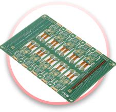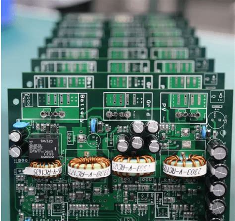
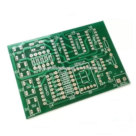
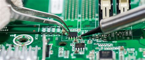
Advanced circuits pcb assembly
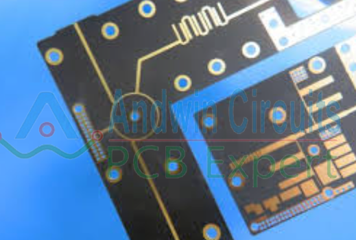
Innovations In Surface Mount Technology For Advanced PCB Assembly
In the rapidly evolving field of electronics, the demand for more compact, efficient, and reliable devices has driven significant advancements in printed circuit board (PCB) assembly.
One of the most notable innovations in this domain is the development and refinement of surface mount technology (SMT).
SMT has revolutionized the way electronic components are mounted onto PCBs, offering numerous advantages over traditional through-hole technology. As we delve into the intricacies of SMT, it becomes evident that its impact on advanced PCB assembly is profound, facilitating the creation of more sophisticated electronic devices.
To begin with, surface mount technology allows for the placement of components directly onto the surface of the PCB, eliminating the need for drilling holes.
This not only reduces the manufacturing time but also enables the use of smaller and lighter components. Consequently, devices can be made more compact, which is particularly beneficial in industries such as consumer electronics, where space is at a premium. Moreover, SMT supports higher component density, allowing for more complex circuits to be integrated into a single board. This capability is crucial for the development of advanced technologies such as smartphones, wearables, and IoT devices, which require intricate circuitry within limited space.
Furthermore, SMT enhances the reliability and performance of electronic assemblies.
The shorter leads used in surface-mounted components reduce parasitic inductance and capacitance, which in turn minimizes signal distortion and improves high-frequency performance. This is particularly advantageous in applications requiring high-speed data transmission and precision, such as telecommunications and aerospace. Additionally, the automated nature of SMT assembly processes ensures consistent quality and reduces the likelihood of human error, further bolstering the reliability of the final product.
Transitioning to the economic aspects, SMT has also contributed to cost efficiencies in PCB assembly.
The automation of the assembly process not only accelerates production but also reduces labor costs. Additionally, the ability to place components on both sides of the PCB maximizes the use of available space, potentially reducing the number of layers required in multilayer boards. This can lead to significant cost savings in materials and manufacturing. As a result, companies can produce more affordable electronic products without compromising on quality or performance.
Despite these advantages, the implementation of SMT in advanced PCB assembly is not without its challenges.
The miniaturization of components necessitates precise placement and soldering techniques, requiring sophisticated equipment and skilled personnel. Moreover, the inspection and testing of SMT assemblies can be more complex due to the higher component density and reduced visibility of solder joints. However, ongoing innovations in inspection technologies, such as automated optical inspection (AOI) and X-ray inspection, are addressing these challenges, ensuring that SMT assemblies meet stringent quality standards.
In conclusion, surface mount technology has undeniably transformed the landscape of advanced PCB assembly. By enabling the production of smaller, more efficient, and reliable electronic devices, SMT has become an indispensable tool in the electronics industry. As technology continues to advance, further innovations in SMT are anticipated, promising even greater enhancements in PCB assembly processes. These developments will undoubtedly pave the way for the next generation of electronic devices, meeting the ever-growing demands of consumers and industries alike.
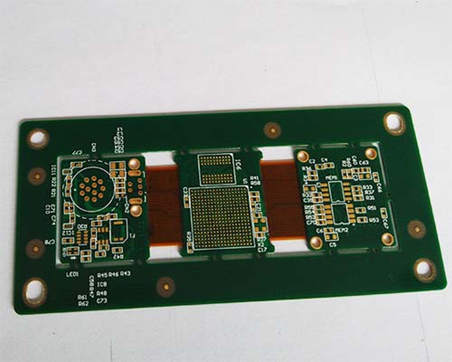
Challenges And Solutions In High-Density Interconnect PCB Design
In the realm of advanced circuits, the design and assembly of high-density interconnect (HDI) printed circuit boards (PCBs) present a unique set of challenges that require innovative solutions. As electronic devices continue to shrink in size while increasing in functionality, the demand for HDI PCBs has surged. These PCBs are characterized by their ability to accommodate a higher number of interconnections in a smaller area, which is essential for modern electronics such as smartphones, tablets, and wearable devices. However, the complexity of HDI PCB design introduces several challenges that must be addressed to ensure optimal performance and reliability.
One of the primary challenges in HDI PCB design is managing the intricate routing of traces.
As the density of components increases, the available space for routing decreases, making it difficult to maintain signal integrity. To overcome this, designers often employ advanced techniques such as microvias, which are smaller than traditional vias and allow for more efficient use of space. Additionally, the use of blind and buried vias can help in creating multi-layer connections without compromising the board’s surface area. These techniques, while effective, require precise manufacturing processes to ensure that the vias are correctly formed and do not introduce defects.
Another significant challenge is thermal management.
As components are packed more densely, the heat generated by the electronic components can lead to performance degradation or even failure if not properly managed. To address this, designers must carefully consider the thermal properties of the materials used in the PCB and incorporate features such as thermal vias and heat sinks. Moreover, advanced simulation tools can be employed during the design phase to predict thermal behavior and optimize the layout accordingly. This proactive approach helps in mitigating potential thermal issues before they manifest in the final product.
Signal integrity is also a critical concern in HDI PCB design.
The close proximity of traces can lead to issues such as crosstalk and electromagnetic interference (EMI), which can adversely affect the performance of the circuit. To combat these issues, designers can utilize differential signaling and controlled impedance techniques. Additionally, incorporating ground planes and shielding can further enhance signal integrity by reducing the impact of external noise. These strategies require a deep understanding of electromagnetic theory and careful planning during the design phase to be effective.
Furthermore, the choice of materials plays a crucial role in the success of HDI PCB design.
The materials must not only support the electrical and thermal requirements but also be compatible with the manufacturing processes. High-performance laminates and substrates are often used to meet these demands, but they can be costly. Therefore, a balance must be struck between performance and cost, which requires careful consideration and expertise.
In conclusion, while the challenges in high-density interconnect PCB design are significant, they are not insurmountable. Through the use of advanced design techniques, careful material selection, and thorough testing, these challenges can be effectively addressed. As technology continues to evolve, the demand for HDI PCBs will only increase, driving further innovation in design and manufacturing processes. By staying at the forefront of these developments, designers and manufacturers can ensure that they meet the ever-growing needs of the electronics industry, delivering products that are both high-performing and reliable.

The Role Of Automated Optical Inspection In Ensuring PCB Quality
In the realm of advanced circuits and printed circuit board (PCB) assembly, ensuring the quality and reliability of the final product is paramount. As electronic devices become increasingly complex, the demand for precision in PCB manufacturing has never been higher. One of the critical technologies that have emerged to meet this demand is Automated Optical Inspection (AOI). AOI plays a pivotal role in maintaining the quality of PCBs by providing a non-invasive, efficient, and accurate method of inspection.
To begin with, AOI systems utilize high-resolution cameras and sophisticated algorithms to capture and analyze images of PCBs.
This technology allows for the rapid detection of defects such as soldering errors, component misalignments, and surface irregularities. By comparing the captured images against a predefined set of standards or a golden board, AOI systems can identify discrepancies with remarkable precision. This capability is particularly crucial in advanced circuits, where even the smallest defect can lead to significant performance issues or complete device failure.
Moreover, the integration of AOI into the PCB assembly process offers several advantages over traditional manual inspection methods.
Manual inspection is not only time-consuming but also prone to human error, especially as the complexity of PCBs increases. In contrast, AOI provides a consistent and repeatable inspection process, significantly reducing the likelihood of defects going unnoticed. This consistency is essential in high-volume production environments, where maintaining a high throughput without compromising quality is a constant challenge.
In addition to improving inspection accuracy, AOI systems contribute to the overall efficiency of the PCB assembly process.
By identifying defects early in the production line, AOI allows for immediate corrective actions, thereby minimizing the risk of defective products reaching the final stages of assembly. This early detection capability not only saves time and resources but also enhances the overall yield of the manufacturing process. Consequently, manufacturers can achieve higher levels of productivity and cost-effectiveness, which are critical in today’s competitive electronics market.
Furthermore, AOI systems are continually evolving, incorporating advancements in machine learning and artificial intelligence to enhance their capabilities.
These technologies enable AOI systems to learn from past inspections, improving their ability to detect subtle defects and adapt to new design variations. As a result, AOI systems are becoming increasingly adept at handling the complexities of modern PCB designs, which often feature miniaturized components and intricate layouts.
Despite the numerous benefits of AOI, it is important to recognize that it is not a standalone solution.
AOI is most effective when integrated into a comprehensive quality assurance strategy that includes other inspection methods such as X-ray inspection and functional testing. By combining these techniques, manufacturers can ensure a more thorough evaluation of PCB quality, addressing both visible and hidden defects.
In conclusion, Automated Optical Inspection is an indispensable tool in the quest for high-quality PCB assembly. Its ability to provide accurate, efficient, and consistent inspection makes it a cornerstone of modern electronics manufacturing. As technology continues to advance, the role of AOI in ensuring PCB quality will undoubtedly expand, further solidifying its position as a critical component of the manufacturing process. By embracing AOI and integrating it with other quality assurance measures, manufacturers can meet the ever-growing demands for reliability and performance in advanced circuits.
Emerging Trends In Flexible And Rigid-Flex PCB Assemblies
In recent years, the electronics industry has witnessed significant advancements in the design and manufacturing of printed circuit boards (PCBs), particularly in the realm of flexible and rigid-flex PCB assemblies. These innovations are driven by the increasing demand for compact, lightweight, and versatile electronic devices that can accommodate the complex requirements of modern technology. As a result, flexible and rigid-flex PCBs have emerged as pivotal components in a wide array of applications, ranging from consumer electronics to aerospace and medical devices.
Flexible PCBs, as the name suggests, are designed to bend and flex, allowing for greater versatility in device design.
This flexibility is achieved through the use of materials such as polyimide or polyester, which provide the necessary durability and resilience. The ability to conform to various shapes and spaces makes flexible PCBs ideal for applications where space is at a premium or where the device must endure mechanical stress. For instance, in wearable technology, flexible PCBs enable the integration of electronic components into clothing or accessories, providing seamless functionality without compromising comfort or aesthetics.
On the other hand, rigid-flex PCBs combine the best of both worlds by integrating flexible circuits with rigid sections.
This hybrid approach offers enhanced reliability and performance, as it allows for the incorporation of multiple layers and complex circuitry within a single board. Rigid-flex PCBs are particularly advantageous in applications that require a high degree of precision and durability, such as in military and aerospace equipment. The ability to withstand extreme conditions and maintain functionality over extended periods makes rigid-flex PCBs a preferred choice for mission-critical applications.
As the demand for more sophisticated electronic devices continues to grow, several emerging trends are shaping the future of flexible and rigid-flex PCB assemblies.
One such trend is the miniaturization of components, which is driving the need for even more compact and efficient PCB designs. Advances in materials science and manufacturing techniques are enabling the production of thinner and lighter PCBs without sacrificing performance. This trend is particularly evident in the development of next-generation smartphones and tablets, where every millimeter of space is meticulously optimized.
Another significant trend is the increasing integration of advanced technologies such as the Internet of Things (IoT) and artificial intelligence (AI) into electronic devices.
These technologies require PCBs that can support high-speed data transmission and complex processing capabilities. Flexible and rigid-flex PCBs are well-suited to meet these demands, as they can accommodate the intricate circuitry and connectivity required for IoT and AI applications. Moreover, the ability to integrate sensors and other components directly onto the PCB enhances the overall functionality and efficiency of the device.
Sustainability is also becoming a key consideration in the design and manufacturing of PCBs.
As environmental concerns continue to rise, there is a growing emphasis on developing eco-friendly materials and processes. Flexible and rigid-flex PCBs offer several advantages in this regard, as they often require fewer raw materials and generate less waste compared to traditional rigid PCBs. Additionally, advancements in recycling and disposal methods are helping to minimize the environmental impact of PCB production and end-of-life management.
In conclusion, the landscape of flexible and rigid-flex PCB assemblies is rapidly evolving, driven by the need for more compact, efficient, and sustainable electronic solutions. As these trends continue to unfold, they will undoubtedly pave the way for new innovations and applications, further solidifying the role of flexible and rigid-flex PCBs in the future of electronics.