Advanced PCB Assembly and Soldering for Reliable Electronics Manufacturing

Key Takeaways
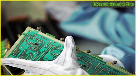
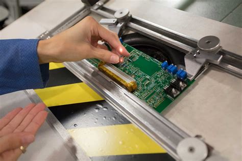
Modern PCB assembly processes leverage automation to achieve unprecedented levels of precision and repeatability, reducing human error while accelerating production timelines. By integrating PCBA (Printed Circuit Board Assembly) solutions such as surface-mount technology (SMT), manufacturers can accommodate increasingly compact designs without compromising functionality. Advanced soldering techniques—including reflow and selective soldering—ensure consistent electrical connections, critical for high-frequency or high-power applications.
Quality control protocols, such as automated optical inspection (AOI) and X-ray testing, play a pivotal role in identifying defects early, safeguarding the reliability of end products. Additionally, rigorous PCB reliability testing—thermal cycling, vibration analysis, and humidity exposure—validates performance under extreme conditions. Effective thermal management strategies, like using thermally conductive substrates or heat-dissipating layouts, further enhance longevity in demanding environments.
The adoption of advanced materials, such as high-temperature laminates and halogen-free substrates, supports durability while aligning with evolving environmental regulations. As the industry evolves, innovations like AI-driven assembly lines and IoT-enabled process monitoring are set to redefine PCB manufacturing, balancing efficiency with sustainability. These foundational elements collectively ensure that modern electronics meet both technical and market demands seamlessly.
Automated PCB Assembly Process Benefits
Modern PCB assembly workflows leverage automation to address the challenges of scalability and precision in electronics manufacturing. By integrating robotic placement systems and AI-driven inspection tools, PCBA production achieves sub-10-micron accuracy, minimizing human error while boosting throughput. Automated lines excel in handling high-volume orders, with pick-and-place machines assembling surface-mount devices (SMDs) at speeds exceeding 25,000 components per hour.
Tip: For optimal results, pair automated PCB assembly with real-time process monitoring to detect soldering anomalies or component misalignments during production.
The transition to automation also enhances repeatability—critical for applications requiring ISO-certified manufacturing standards. Closed-loop feedback systems adjust parameters like solder paste deposition and reflow oven temperatures dynamically, ensuring consistent joint quality across batches. This approach reduces rework rates by up to 60% compared to manual methods, particularly when assembling complex boards with fine-pitch ICs or ball grid array (BGA) components.
Furthermore, automated PCBA processes integrate seamlessly with digital traceability protocols, enabling manufacturers to track each board’s production history—a vital feature for aerospace and medical device compliance. By combining speed with zero-defect methodologies, these systems future-proof manufacturing workflows against evolving miniaturization demands.
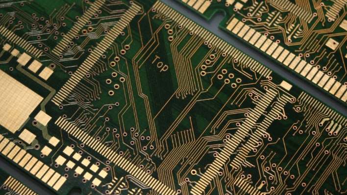
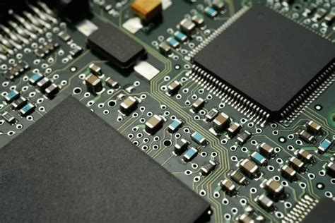
Surface-Mount Technology for Compact Designs
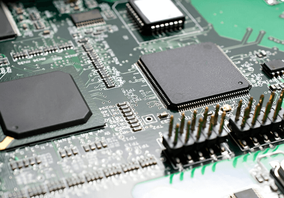
Modern PCB assembly processes increasingly rely on surface-mount technology (SMT) to meet the demand for smaller, high-performance electronic devices. Unlike traditional through-hole methods, SMT enables the placement of miniaturized components directly onto the board’s surface, reducing overall footprint while maximizing circuit density. This approach is critical for applications like wearables, IoT sensors, and medical devices, where space constraints and weight limitations are paramount.
A key advantage of SMT in PCBA workflows is its compatibility with automated production systems. Pick-and-place machines equipped with vision systems can position components as small as 01005 packages (0.4 mm × 0.2 mm) with micron-level accuracy, ensuring consistent placement across high-volume batches. Post-placement, reflow soldering creates reliable electrical connections by melting solder paste in controlled thermal profiles, minimizing thermal stress on sensitive parts.
| SMT vs. Through-Hole Comparison | |
|---|---|
| Component Size | Submillimeter-scale vs. larger leads |
| Placement Density | 2–3x higher component density |
| Thermal Performance | Reduced thermal mass improves heat dissipation |
| Typical Applications | Consumer electronics, aerospace, automotive |
To ensure reliability, designers must address challenges like tombstoning (uneven component lifting) and solder bridging, often mitigated through optimized stencil designs and solder paste formulations. As PCB assembly evolves, SMT continues to enable thinner, lighter, and more energy-efficient designs without compromising performance—a cornerstone of next-generation electronics manufacturing.
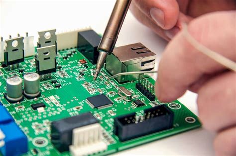
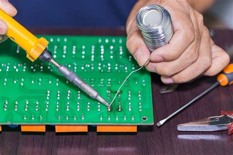
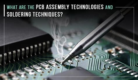
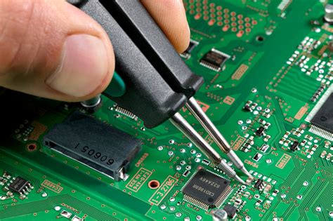
Precision Soldering Techniques Explained
Modern PCB assembly relies on precision soldering to ensure electrical connectivity and mechanical stability in compact, high-density designs. Reflow soldering, a cornerstone of PCBA workflows, uses controlled heating profiles to melt solder paste, creating uniform joints across surface-mount components. For through-hole components, wave soldering remains critical, though advancements like selective soldering enable targeted application, minimizing thermal stress on sensitive parts. Automated optical inspection (AOI) systems validate joint quality, detecting defects like cold solder joints or bridging with micron-level accuracy.
The shift to lead-free solder alloys, driven by environmental regulations, demands tighter process controls. Temperature gradients must align with material specifications to prevent warping or delamination. In mixed-technology boards, laser soldering provides localized heat application, ideal for fine-pitch components or heat-sensitive substrates. Manufacturers also leverage nitrogen-rich atmospheres during soldering to reduce oxidation, enhancing joint durability.
These techniques directly influence PCB reliability, especially in aerospace or medical devices where failure is not an option. By integrating real-time monitoring and adaptive algorithms, PCBA systems self-correct parameters like solder volume or heating duration, ensuring consistency across high-volume production runs. This precision bridges the gap between design intent and functional electronics, setting the stage for rigorous quality control protocols discussed next.
Quality Control in Electronics Manufacturing
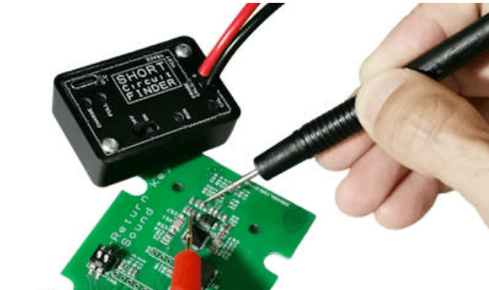
Effective PCB assembly processes rely on rigorous quality control measures to ensure the integrity of electronic devices. During PCBA (Printed Circuit Board Assembly), manufacturers implement multi-stage inspection protocols to identify defects in solder joints, component placement, and material integrity. Advanced tools like automated optical inspection (AOI) and X-ray imaging scrutinize micro-scale features, detecting issues such as cold solder joints or misaligned surface-mount devices (SMDs).
Statistical process control (SPC) systems analyze production data in real time, enabling adjustments to soldering temperatures or stencil printing parameters. For mission-critical applications, cross-sectional analysis verifies internal layer connections, while environmental stress testing simulates operational conditions to validate long-term reliability.
A robust quality framework also includes adherence to international standards like IPC-A-610 for acceptability criteria and ISO 9001 for process consistency. By integrating these protocols into PCB assembly workflows, manufacturers minimize failure rates and ensure compliance with industry-specific requirements—from automotive-grade durability to medical device safety. This systematic approach bridges precision manufacturing with end-user demands for high-performance electronics.
PCB Reliability Testing Methods
Ensuring long-term performance in modern PCB assembly requires rigorous reliability testing protocols. These methods validate whether assembled boards can withstand operational stresses, environmental factors, and aging effects. Key tests include thermal cycling to simulate temperature fluctuations, vibration testing for mechanical durability, and HAST (Highly Accelerated Stress Testing) to assess moisture resistance. For PCBA products intended for aerospace or automotive applications, electrical continuity checks and solder joint integrity analysis are prioritized to prevent field failures.
Advanced testing integrates automated optical inspection (AOI) systems with machine learning algorithms to detect micro-cracks or voids in solder connections—defects often invisible to manual inspection. Additionally, accelerated life testing compresses years of usage into weeks, providing data on mean time between failures (MTBF). These protocols are critical in PCB assembly workflows, as they bridge quality control and end-user reliability, ensuring compliance with industry standards like IPC-6012 and MIL-PRF-31032. By combining empirical data with predictive modeling, manufacturers preemptively address weaknesses in PCBA designs, reducing costly recalls and enhancing product lifecycle performance.
Thermal Management in Circuit Boards
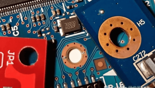
Effective thermal management in high-density electronics is critical for maintaining PCB assembly reliability, particularly in applications involving power-intensive components or extended operational cycles. As PCBA designs grow more compact, heat dissipation challenges intensify due to reduced airflow and increased component proximity. Engineers employ multi-layered thermal strategies, integrating thermal vias and copper pours to distribute heat evenly across the board. Advanced metal-core substrates and ceramic-filled laminates further enhance thermal conductivity, minimizing hotspots that could compromise solder joint integrity.
Automated PCB assembly systems now incorporate real-time thermal profiling during reflow soldering, ensuring optimal temperature gradients for lead-free solder alloys. Post-production, PCBA validation often includes infrared thermography to identify thermal anomalies undetectable through visual inspection. For mission-critical systems, active cooling solutions such as embedded heat pipes or microfluidic channels are increasingly paired with surface-mount technology, balancing miniaturization with thermal efficiency. These innovations underscore the industry’s shift toward proactive thermal design rather than reactive mitigation, aligning with demands for durable, high-performance electronics in aerospace, automotive, and IoT applications.
Advanced Materials for Durable PCBs
The longevity and performance of modern electronics hinge on the materials used in PCB assembly and PCBA workflows. Innovations in substrate laminates, such as high-frequency Rogers 4350B or halogen-free FR-4 variants, provide enhanced thermal stability and signal integrity, critical for high-power or high-speed applications. These materials reduce dielectric losses while resisting warping under extreme temperatures, a common challenge in precision soldering processes.
For conductive layers, copper alloys with organic solderability preservatives (OSP) or immersion silver finishes offer superior oxidation resistance, ensuring reliable electrical connections during surface-mount technology integration. Advanced ceramic-filled prepregs further bolster multilayer PCB durability by minimizing delamination risks in humid environments.
In demanding industries like automotive or aerospace, polyimide flex materials enable lightweight, bendable circuits without compromising structural integrity. Pairing these with lead-free solder pastes containing nano-sized silver particles enhances joint reliability in automated PCB assembly lines. As manufacturers prioritize sustainability, bio-based substrates and recyclable metal cores are gaining traction, aligning quality control standards with eco-design principles.
By leveraging these material advancements, PCBA providers can deliver circuit boards that withstand mechanical stress, thermal cycling, and prolonged operational demands—key factors in achieving zero-defect manufacturing benchmarks.
Future Trends in PCB Manufacturing
The evolution of PCB assembly and PCBA processes is being reshaped by emerging technologies aimed at addressing demands for miniaturization, sustainability, and higher operational frequencies. Industry leaders are increasingly adopting additive manufacturing techniques, such as 3D-printed circuitry, to enable complex geometries while reducing material waste. Concurrently, the integration of flexible hybrid electronics (FHE) is expanding applications in wearable devices and IoT systems, requiring novel approaches to soldering and substrate bonding.
Another transformative trend lies in AI-driven process optimization, where machine learning algorithms analyze PCB assembly data in real time to predict solder joint defects or component misalignments. This shift complements advancements in eco-friendly manufacturing, with biodegradable substrates and lead-free solder alloys gaining traction. For PCBA workflows, autonomous robotic systems are enhancing precision in component placement, particularly for ultra-fine-pitch ICs and micro-BGA packages.
Thermal management solutions are also evolving, with embedded cooling channels and graphene-based heat spreaders becoming critical for high-power applications. As 5G and automotive electronics push signal integrity requirements, manufacturers are prioritizing low-loss dielectric materials and embedded passive components to minimize interference. These innovations, combined with Industry 4.0 integration, position PCB assembly as a cornerstone of next-generation smart manufacturing ecosystems.
Conclusion
The evolution of PCB assembly and soldering technologies underscores their pivotal role in delivering high-performance electronic systems. As the electronics industry demands greater miniaturization and functionality, PCBA processes have adapted through innovations like laser-assisted soldering and automated optical inspection. These advancements not only enhance precision but also address critical challenges in thermal management and material compatibility, ensuring boards withstand harsh operating conditions.
By integrating automated PCB assembly with rigorous reliability testing, manufacturers achieve consistent results while minimizing defects. The shift toward lead-free soldering alloys and high-temperature substrates further demonstrates the sector’s commitment to sustainability and durability. Looking ahead, the convergence of AI-driven process optimization and advanced surface-mount technology will continue to redefine production benchmarks, enabling faster prototyping and scalable solutions.
Ultimately, the success of modern electronics hinges on balancing cutting-edge techniques with meticulous quality control—a principle that remains central to PCB assembly excellence. As industry standards evolve, manufacturers must prioritize adaptability to maintain competitiveness in an increasingly dynamic market.
FAQs
What distinguishes PCB assembly from PCBA?
PCB assembly refers to the process of populating a bare circuit board with components, while PCBA (Printed Circuit Board Assembly) denotes the completed board with all components soldered and tested. The latter includes both assembly and quality verification stages.
How does automated assembly improve manufacturing consistency?
Automated assembly systems use precision robotics to place surface-mount devices (SMDs) with micron-level accuracy, minimizing human error. This ensures uniform solder joint quality and repeatability, critical for high-volume PCBA production.
Why is surface-mount technology preferred for compact designs?
Surface-mount technology (SMT) allows smaller components to be placed directly onto the board’s surface, enabling higher component density. This method supports advanced PCB assembly for devices like wearables and IoT sensors.
What quality control steps are essential in PCBA?
Post-soldering inspections, such as automated optical inspection (AOI) and X-ray testing, identify defects like solder bridges or misaligned components. Functional testing also validates the board’s electrical performance before deployment.
How do thermal management practices enhance PCB reliability?
Techniques like using thermally conductive substrates or adding heat sinks dissipate excess heat, preventing component degradation. This is vital for PCB assembly in high-power applications like automotive electronics.
Optimize Your Next PCBA Project Today
For tailored solutions in advanced PCB assembly and soldering, please click here to consult our engineering team. Explore how our expertise in precision soldering and reliability testing can streamline your production workflow.