Advanced PCB Assembly Strategies for Streamlined Electronics Production
Key Takeaways
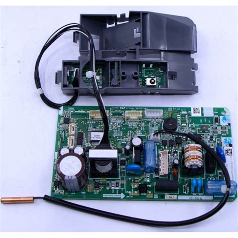
Modern PCB assembly processes prioritize design optimization to accommodate high-density interconnects and miniaturized components, enabling compact yet powerful electronic devices. The integration of automated assembly lines ensures precision component placement at scale, reducing human error while accelerating production cycles. Strategic material selection—including high-performance substrates and advanced solder alloys—plays a critical role in enhancing thermal management and signal integrity, particularly for applications requiring high-reliability outcomes. Rigorous testing protocols, such as automated optical inspection (AOI) and in-circuit testing (ICT), are now indispensable for identifying defects early, ensuring compliance with stringent quality standards.
Scalable PCBA workflows leverage modular production models to adapt swiftly to fluctuating demand, balancing cost-efficiency with rapid turnaround times. Innovations like surface-mount technology (SMT) and 3D-printed circuitry further streamline fabrication, minimizing waste and material costs in large-scale PCB fabrication. Emerging trends, such as AI-driven process optimization and IoT-enabled monitoring systems, are reshaping electronics manufacturing, offering predictive analytics to preempt bottlenecks. By combining cost-effective workflows with cutting-edge technologies, manufacturers achieve faster time-to-market without compromising on performance, solidifying PCB assembly as the backbone of modern electronics production.
The Evolution of PCB Assembly in Modern Electronics Manufacturing
The transition from rudimentary PCB assembly methods to today’s highly sophisticated processes underscores the rapid advancements in electronics manufacturing. Early PCBA (printed circuit board assembly) workflows relied heavily on manual soldering and through-hole components, limiting both precision and scalability. However, the rise of surface-mount technology (SMT) revolutionized the industry by enabling smaller, denser designs and automated placement of micro-components. Modern PCB assembly now integrates advanced robotics, AI-driven inspection systems, and high-speed pick-and-place machines to achieve sub-micron accuracy, ensuring consistent quality even in high-density circuit board configurations.
Material innovation has further propelled this evolution. Engineers now prioritize substrates with enhanced thermal conductivity and signal integrity, such as polyimide flex circuits or ceramic-filled laminates, to meet the demands of 5G, IoT, and aerospace applications. Additionally, the adoption of design-for-manufacturing (DFM) principles ensures that layouts are optimized for automated assembly, minimizing defects and rework.
Tip: To maximize yield in PCBA projects, collaborate early with fabrication partners to align design choices with production capabilities.
The shift toward smart factories has also introduced real-time monitoring and adaptive workflows, allowing manufacturers to swiftly adjust to fluctuating demand. Technologies like automated optical inspection (AOI) and X-ray testing now provide non-destructive quality validation, reducing failure rates in mission-critical applications. These advancements not only streamline electronics production but also lower costs through waste reduction and improved resource allocation. As PCB assembly continues to evolve, its role as the backbone of modern electronics remains unchallenged, driving innovation across industries from consumer tech to renewable energy systems.
Design Optimization for High-Density Circuit Board Configurations
Modern electronics demand increasingly compact yet powerful devices, driving the need for high-density circuit board configurations. Optimizing designs for these complex layouts requires balancing component density, signal integrity, and thermal management. A critical first step involves leveraging advanced PCB assembly (PCBA) techniques such as microvia technology and stacked via structures, which minimize space consumption while maintaining electrical performance. These methods enable designers to accommodate more components per unit area, essential for applications like IoT devices and wearable technology.
Material selection plays a pivotal role in high-density designs. Using low-CTE (coefficient of thermal expansion) substrates reduces mechanical stress during thermal cycling, while high-Tg (glass transition temperature) laminates enhance reliability under elevated temperatures. Additionally, integrating embedded passive components directly into the board substrate eliminates surface-mounted parts, freeing space for active components.
| Design Consideration | Traditional Approach | Optimized High-Density Strategy |
|---|---|---|
| Trace Width | 5-8 mil | 3-4 mil with laser-drilled microvias |
| Layer Count | 6-8 layers | 10+ layers with staggered via placement |
| Thermal Management | External heat sinks | Embedded thermal vias + conductive pads |
| Testing | Manual inspection | Automated optical inspection (AOI) + X-ray |
To ensure signal integrity in densely packed layouts, impedance-controlled routing and differential pair alignment are prioritized. Simulation tools like 3D electromagnetic field solvers predict interference patterns, allowing pre-production adjustments. Proactive design-for-manufacturing (DFM) checks further reduce errors, ensuring compatibility with automated PCBA workflows.
Thermal challenges escalate with component density. Strategies such as copper-filled vias and thermal interface materials (TIMs) dissipate heat efficiently, preventing hotspots. For power-hungry applications, multiphase power delivery networks distribute current evenly, reducing resistive losses.
Finally, collaboration between design and manufacturing teams is critical. By aligning high-density PCB assembly requirements with production capabilities, manufacturers achieve scalable, repeatable outcomes. This synergy minimizes rework, accelerates time-to-market, and ensures that high-reliability PCBA meets the stringent demands of modern electronics.
Automated Assembly Lines: Precision and Speed in Component Placement
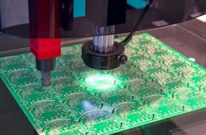
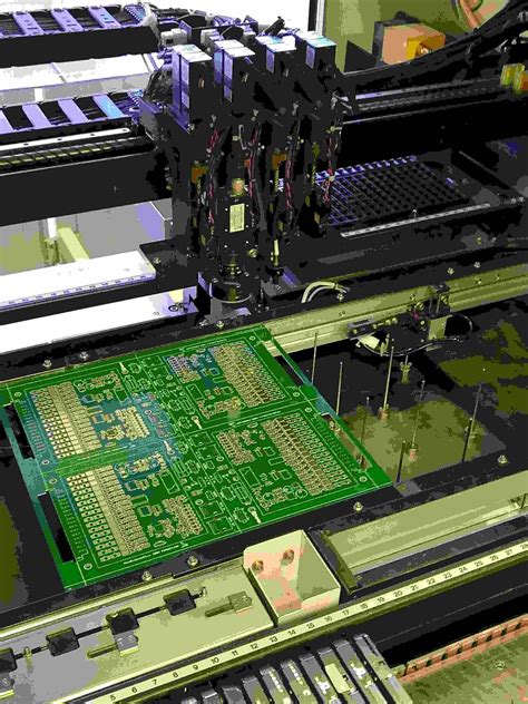
Modern PCB assembly processes rely heavily on automated systems to achieve unprecedented levels of precision and efficiency in component placement. Advanced pick-and-place machines, equipped with high-resolution vision systems and AI-driven alignment algorithms, enable rapid, error-free positioning of micro-scale components—even those smaller than 01005 packages. These systems operate at speeds exceeding 50,000 placements per hour, minimizing human intervention while ensuring sub-10-micron accuracy. By integrating PCBA workflows with real-time data analytics, manufacturers can dynamically adjust placement parameters, reducing defects caused by thermal expansion or solder paste inconsistencies.
The adoption of closed-loop feedback mechanisms further enhances quality control, allowing immediate correction of misaligned components during the assembly process. For high-density designs, multi-head gantry systems and dual-lane conveyors optimize throughput without compromising placement precision. Additionally, modular automation platforms enable seamless scalability, supporting both low-mix/high-volume and high-mix/low-volume production demands. Advanced solder paste inspection (SPI) and automated optical inspection (AOI) tools work in tandem with assembly lines to flag anomalies early, preventing costly rework downstream.
Material handling innovations, such as tape-and-reel feeders with predictive replenishment alerts, ensure uninterrupted production cycles. Meanwhile, adaptive nozzle changers on placement machines allow rapid switching between component types, critical for mixed-technology boards combining surface-mount (SMT) and through-hole (THT) parts. These advancements not only accelerate time-to-market but also reduce waste by optimizing material usage. As PCB assembly evolves, the synergy between robotics, machine learning, and IoT-enabled monitoring continues to redefine manufacturing benchmarks, delivering high-reliability outcomes essential for aerospace, medical devices, and next-gen consumer electronics.
Material Selection Strategies for Enhanced Thermal and Electrical Performance
Effective PCB assembly relies heavily on selecting materials that balance thermal management and electrical efficiency, particularly in high-performance applications. Modern PCBA processes demand substrates, laminates, and conductive materials capable of withstanding elevated operating temperatures while minimizing signal loss. For instance, high-Tg (glass transition temperature) laminates are increasingly adopted to maintain structural integrity in environments where heat dissipation is critical, such as in automotive or industrial electronics. These materials reduce the risk of delamination during reflow soldering, ensuring long-term reliability.
Thermally conductive dielectric materials, such as metal-core substrates or ceramic-filled polymers, are prioritized for applications requiring rapid heat transfer. These substrates enhance thermal conductivity by up to 10x compared to traditional FR-4, directly improving the lifespan of power-dense components like ICs or LEDs. Additionally, advanced copper alloys with low oxidation rates are employed to optimize electrical performance, reducing resistive losses in high-current pathways.
For high-frequency circuits, low-loss dielectrics like polyimide or PTFE-based laminates minimize signal attenuation, ensuring consistent impedance control. Pairing these with silver or gold finishes on contact surfaces further enhances conductivity while resisting corrosion. In multilayer PCBA designs, material compatibility between layers is critical—hybrid stack-ups combining rigid and flexible materials enable compact, heat-resistant configurations without compromising signal integrity.
Emerging trends also emphasize sustainability, with halogen-free laminates and recyclable substrates gaining traction. These materials meet stringent environmental regulations while maintaining performance benchmarks. By aligning material selection with thermal and electrical requirements, manufacturers achieve scalable, cost-effective production workflows without sacrificing quality. This strategic approach ensures that PCB assembly processes remain adaptable to evolving technological demands, from consumer IoT devices to aerospace-grade systems.
Advanced Testing Protocols for Quality Assurance and Reliability
Modern PCB assembly processes demand rigorous advanced testing protocols to ensure both quality and long-term reliability in electronic systems. As high-density designs and miniaturized components become standard, manufacturers rely on a combination of automated and data-driven inspection methods to identify defects early. Automated Optical Inspection (AOI) systems, for instance, use high-resolution cameras and machine vision algorithms to detect soldering flaws, misaligned components, or missing parts in PCBA units. Complementing this, In-Circuit Testing (ICT) validates electrical performance by checking connectivity, resistance, and capacitance values against design specifications, ensuring functional integrity before products leave the production line.
For mission-critical applications, Environmental Stress Screening (ESS) subjects assemblies to extreme temperatures, vibrations, and humidity cycles, simulating real-world operating conditions to uncover latent failures. Additionally, functional testing replicates end-use scenarios, verifying that the assembled board operates as intended within its target system. Emerging tools like predictive analytics and AI-powered defect classification further enhance accuracy by analyzing historical production data to anticipate potential failure modes and refine testing parameters dynamically.
To address the complexities of mixed-technology assemblies (combining surface-mount and through-hole components), X-ray inspection provides non-destructive internal imaging, identifying hidden issues such as voiding in solder joints or layer misalignment in multi-layered boards. These protocols not only reduce rework costs but also align with industry standards like IPC-A-610, ensuring compliance across global supply chains. By integrating these strategies into scalable PCB assembly workflows, manufacturers achieve higher first-pass yields while maintaining traceability—a critical factor for industries requiring stringent reliability, such as aerospace, medical devices, and automotive electronics.
Scalable Production Models for Flexible Manufacturing Demands
Modern electronics manufacturing demands PCB assembly processes that adapt seamlessly to shifting market needs while maintaining rigorous quality standards. Scalable production models leverage modular assembly systems and PCBA-optimized workflows to address both high-volume orders and specialized low-to-mid volume runs. By integrating automated component placement with reconfigurable production lines, manufacturers achieve rapid scalability without compromising precision or throughput. Key strategies include hybrid manufacturing setups that combine surface-mount technology (SMT) with flexible robotic systems, enabling quick transitions between product variants or design iterations.
Central to scalable models is the adoption of data-driven resource allocation, where real-time analytics optimize material usage, machine uptime, and labor efficiency. For instance, dynamic scheduling algorithms adjust task prioritization based on order urgency or component availability, minimizing bottlenecks in multi-stage PCB assembly workflows. Additionally, cloud-based inventory management synchronizes with PCBA production lines to ensure just-in-time delivery of critical parts, reducing warehousing costs and obsolescence risks.
To address fluctuating demand, manufacturers increasingly deploy agile manufacturing cells that support parallel processing of diverse board types. These cells utilize standardized interfaces for tooling and testing equipment, allowing rapid reconfiguration for new projects. Advanced thermal profiling and solder paste inspection (SPI) systems further enhance adaptability by auto-adjusting parameters for varying board geometries or material specifications. Such flexibility is critical for industries like IoT, automotive, and medical devices, where product lifecycles are compressed and customization is paramount.
By embracing scalable PCB assembly frameworks, companies achieve cost-effective responsiveness—balancing economies of scale with the agility to pivot production in response to market shifts. This approach not future-proofs manufacturing operations but also aligns with sustainability goals by minimizing overproduction and material waste.
Cost-Effective Workflows in Large-Scale PCB Fabrication
Achieving cost efficiency in high-volume PCB assembly requires a strategic blend of process optimization, advanced automation, and intelligent resource management. Modern PCBA workflows leverage design-for-manufacturability (DFM) principles to minimize material waste and reduce production bottlenecks. By analyzing thermal management and signal integrity early in the design phase, manufacturers can avoid costly revisions during fabrication.
A critical driver of cost savings lies in automated assembly lines, where high-speed pick-and-place systems ensure precise component positioning while minimizing human error. These systems, integrated with machine vision and real-time analytics, enable rapid throughput for large batches without sacrificing quality. Additionally, standardized component libraries and panelization techniques optimize material usage, further lowering per-unit costs.
Material selection also plays a pivotal role. Bulk purchasing of high-performance substrates, such as FR-4 or polyimide-based laminates, coupled with strategic partnerships with suppliers, reduces raw material expenses. Advanced PCB assembly workflows also employ just-in-time (JIT) inventory models to mitigate storage costs and obsolescence risks.
For scalability, manufacturers increasingly adopt modular production setups. These systems allow seamless reconfiguration of PCBA lines to accommodate varying product designs or order volumes. Incorporating predictive maintenance protocols ensures equipment uptime, preventing unplanned downtime that disrupts large-scale operations.
Quality assurance is embedded into cost-effective workflows through automated optical inspection (AOI) and in-circuit testing (ICT). These technologies identify defects early, reducing scrap rates and rework costs. By combining these strategies, manufacturers achieve economies of scale while maintaining flexibility to adapt to shifting market demands.
Emerging Technologies Shaping the Future of Electronics Assembly
The rapid evolution of PCB assembly processes is being driven by innovations that prioritize precision, scalability, and adaptability. Central to this transformation are automated optical inspection (AOI) systems, which leverage machine learning algorithms to detect microscopic defects in PCBA units with unprecedented accuracy. These systems reduce human error and enable real-time adjustments during production, ensuring consistent quality across high-volume manufacturing runs. Another breakthrough lies in additive manufacturing techniques, such as 3D-printed conductive traces, which allow for complex, multi-layer circuit designs while minimizing material waste.
Advancements in artificial intelligence (AI) are further refining component placement strategies, with robotic arms equipped with vision systems achieving sub-micron precision in positioning even the smallest surface-mount devices (SMDs). This level of accuracy is critical for high-density interconnect (HDI) boards, where space optimization directly impacts performance. Additionally, the integration of IoT-enabled devices into assembly lines facilitates predictive maintenance, reducing downtime by anticipating equipment failures before they disrupt workflows.
Material science innovations are also reshaping PCB assembly, particularly in thermal management. High-performance substrates with enhanced thermal conductivity are enabling compact designs for power electronics, while low-temperature co-fired ceramics (LTCC) support high-frequency applications in 5G and IoT devices. These materials, combined with advanced soldering techniques like laser reflow, ensure robust electrical connections under extreme operating conditions.
Finally, sustainability is becoming a cornerstone of modern PCBA practices. Manufacturers are adopting lead-free solders and recyclable laminates to meet environmental regulations without compromising reliability. By merging these technologies, the electronics industry is poised to deliver faster, smarter, and more eco-conscious production frameworks, solidifying PCB assembly as a linchpin of next-generation manufacturing.
Conclusion
The integration of advanced PCB assembly strategies has become indispensable for meeting the demands of modern electronics manufacturing. By leveraging innovations in automated component placement and high-precision soldering techniques, manufacturers achieve unparalleled accuracy while reducing production timelines. The adoption of design-for-manufacturing (DFM) principles ensures that high-density circuit boards are optimized for both performance and scalability, minimizing errors during PCBA processes. Additionally, material innovations—such as high-thermal-conductivity substrates and low-loss dielectric laminates—address critical challenges in thermal management and signal integrity, particularly in applications requiring reliability under extreme conditions.
Advanced testing protocols, including automated optical inspection (AOI) and in-circuit testing (ICT), have elevated quality assurance standards, enabling early defect detection and reducing rework costs. Scalable production models further enhance flexibility, allowing seamless transitions between prototyping and high-volume PCB assembly without compromising efficiency. Cost-effective workflows, driven by smart inventory management and lean manufacturing practices, ensure that large-scale PCBA projects remain economically viable while maintaining stringent quality benchmarks.
As emerging technologies like AI-driven process optimization and IoT-enabled production monitoring gain traction, the future of electronics manufacturing will hinge on the continuous refinement of PCB assembly methodologies. By balancing innovation with practicality, industry leaders can deliver solutions that meet evolving market needs while sustaining long-term competitiveness in a dynamic global landscape.
FAQs
What distinguishes PCB assembly from PCBA in modern manufacturing?
PCB assembly refers to the process of populating a bare circuit board with components, while PCBA (Printed Circuit Board Assembly) describes the fully assembled and functional board. Modern techniques emphasize automation and precision to bridge design intent with real-world performance.
How do automated assembly lines enhance PCBA quality?
Automated systems use vision-guided robotics and machine learning algorithms to place components with micron-level accuracy. This reduces human error, accelerates throughput, and ensures consistency in high-density configurations.
What materials optimize thermal management in PCB assembly?
Advanced substrates like high-Tg laminates and metal-core boards dissipate heat efficiently. Pairing these with low-void solder pastes minimizes thermal stress, extending product lifespans in demanding environments.
Can PCBA workflows scale for fluctuating production demands?
Yes. Modular assembly lines and just-in-time inventory systems enable rapid scaling. Manufacturers leverage demand forecasting tools to align capacity with project requirements without compromising speed or quality.
What testing methods ensure reliability in PCB assembly?
Combining automated optical inspection (AOI), X-ray imaging, and in-circuit testing (ICT) identifies defects early. Environmental stress testing further validates performance under extreme conditions.
How do advanced PCBA strategies reduce costs?
Optimized panelization, component standardization, and predictive maintenance minimize waste and downtime. Bulk material procurement and energy-efficient processes further lower per-unit expenses.
Ready to Optimize Your Electronics Production?
Explore tailored PCB assembly solutions that align with your project’s needs. For expert guidance on implementing advanced PCBA strategies, please click here.