Advanced PCB Assembly Techniques Driving Electronics Innovation
Key Takeaways
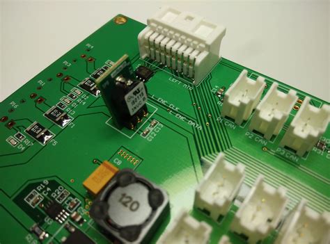
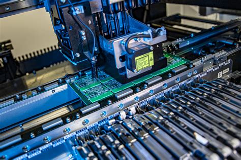
Modern PCB assembly techniques form the backbone of today’s electronics evolution, enabling breakthroughs across industries. Precision manufacturing in PCBA ensures seamless integration of microcomponents, critical for IoT devices requiring ultra-compact designs and energy efficiency. Innovations like automated optical inspection (AOI) and 3D solder paste dispensing enhance reliability, directly supporting AI systems that demand high-speed signal integrity and thermal stability.
In wearable technology, flexible PCB assembly methods allow for lightweight, bendable circuits that conform to ergonomic designs while maintaining durability. Meanwhile, advancements in surface-mount technology (SMT) and multi-layer stacking address the growing complexity of smart devices. These PCBA strategies not only accelerate AI-driven applications but also pave the way for next-gen innovations like edge computing modules and biodegradable substrates. By prioritizing scalability and sustainability, manufacturers are redefining how electronics are built—and how they shape tomorrow’s tech landscape.

Precision PCB Assembly in IoT
The rapid expansion of IoT devices demands unparalleled accuracy in PCB assembly to ensure reliability in compact, energy-efficient designs. Modern high-density interconnect (HDI) techniques enable the placement of microscopic components on multilayer boards, critical for sensors and communication modules in smart environments. PCBA processes now integrate automated optical inspection (AOI) and X-ray verification to detect sub-millimeter defects, reducing failure rates in temperature-sensitive applications like industrial monitoring or wearable health trackers.
"Precision in IoT-focused PCB assembly isn’t just about miniaturization—it’s about balancing durability with signal integrity in unpredictable operating conditions."
Advanced surface-mount technology (SMT) paired with laser-drilled vias supports the creation of ultra-thin, flexible circuits, essential for embedding electronics into unconventional form factors. For instance, PCBA workflows optimized for IoT prioritize low-power consumption layouts, leveraging materials with high thermal conductivity to mitigate heat buildup in confined spaces. Transitioning seamlessly from design to production, manufacturers are adopting AI-driven trace routing algorithms to minimize electromagnetic interference—a key consideration for devices operating in densely connected networks.
As IoT ecosystems evolve, innovations in PCB assembly are also addressing scalability. Modular PCBA approaches allow for rapid customization of sensor arrays and edge-computing nodes, ensuring compatibility with diverse protocols like LoRaWAN or Zigbee. This adaptability positions precision assembly as the backbone of next-gen smart infrastructure, from autonomous agricultural systems to real-time urban energy grids.

AI System PCB Breakthroughs
Recent advancements in PCB assembly (PCBA) are revolutionizing artificial intelligence hardware, enabling faster processing and improved energy efficiency. Modern AI systems demand ultra-high-density interconnects and multi-layer board architectures to support complex neural networks. Innovations like embedded passive components and 3D-printed circuitry are reducing signal latency by up to 40%, critical for real-time AI decision-making.
A key development lies in thermally optimized PCBA designs, which integrate advanced materials like ceramic substrates or flexible polymers to manage heat dissipation in high-performance AI chips. For example:
| Design Feature | AI Application Impact |
|---|---|
| Microvia Stacking | 50% higher component density |
| Copper-filled Trenches | 30% improved thermal conductivity |
| Laser-Drilled Alignment | ±5μm placement accuracy |
These techniques allow PCB assembly providers to meet the rigorous demands of AI training clusters and edge-computing devices. Additionally, automated optical inspection (AOI) systems now leverage machine learning to detect sub-micron defects, ensuring reliability in mission-critical AI infrastructure. As AI algorithms grow more complex, the synergy between PCBA precision and computational power will remain pivotal, driving innovations like neuromorphic computing and autonomous systems.
This progress seamlessly aligns with emerging trends in wearable tech, where miniaturized PCB assembly methods similarly push boundaries in consumer electronics.
Wearable Tech PCB Innovations
The evolution of PCB assembly techniques has become a cornerstone for advancing wearable technology, enabling devices to achieve unprecedented levels of compactness and functionality. Modern PCBA processes now integrate ultra-thin substrates and flexible circuits, allowing engineers to design wearables that conform seamlessly to the human body. Innovations such as embedded sensors and multi-layer stacking are critical for devices like smartwatches and health monitors, which demand high-density layouts without compromising durability.
A key breakthrough lies in the adoption of flexible hybrid electronics (FHE), where PCB assembly methods combine rigid and flexible components to optimize space and performance. This approach supports real-time data processing in fitness trackers and medical wearables, ensuring reliable operation under dynamic physical conditions. Additionally, advancements in laser-direct structuring (LDS) and high-density interconnect (HDI) technologies enhance signal integrity, reducing power consumption while maintaining rapid response times.
To meet the demands of miniaturization, manufacturers are leveraging automated PCBA lines equipped with precision pick-and-place systems and 3D solder paste inspection. These processes ensure microscopic components—such as microcontrollers and wireless modules—are positioned with sub-millimeter accuracy. As wearable tech expands into augmented reality (AR) glasses and biometric clothing, the role of PCB assembly in enabling lightweight, energy-efficient designs will remain pivotal, driving both user comfort and technological capability.

Advanced Electronics Assembly Trends
As electronics evolve toward greater complexity and miniaturization, PCB assembly processes are adapting to meet demands for smarter, smaller devices. The integration of high-density interconnect (HDI) designs and flexible substrates has become pivotal, enabling PCBA solutions to support ultra-compact wearables and AI-driven systems. Manufacturers now prioritize automated optical inspection (AOI) and 3D solder paste inspection to ensure micron-level accuracy, reducing defects in densely packed circuits.
A notable shift is the adoption of multi-material stacking, where hybrid PCB assembly techniques combine rigid and flexible layers to optimize space and durability. This approach is critical for applications like foldable displays and implantable medical devices. Additionally, advancements in thermal management — such as embedded heat sinks and advanced conductive adhesives — address heat dissipation challenges in high-performance computing PCBA.
The rise of modular assembly further accelerates prototyping cycles, allowing seamless integration of IoT sensors or AI accelerators into existing designs. By balancing precision with scalability, these trends underscore how modern PCB assembly methods are redefining the boundaries of electronic innovation.
Smart Device Manufacturing Solutions
Modern PCB assembly techniques are revolutionizing how smart devices are designed and produced, balancing miniaturization demands with enhanced functionality. As consumer expectations shift toward compact yet powerful gadgets, PCBA (Printed Circuit Board Assembly) processes now integrate laser-direct imaging for micron-level accuracy and automated optical inspection (AOI) systems to eliminate microfaults. These advancements enable manufacturers to embed multi-sensor arrays and low-power communication modules into devices as slim as 3mm while maintaining thermal efficiency.
A key innovation lies in mixed-material substrates combining rigid and flexible PCB assembly layers, allowing seamless integration in foldable displays or curved wearables. For industrial IoT edge devices, PCBA workflows utilize high-density interconnect (HDI) boards to support real-time data processing without compromising durability. Transitioning from earlier sections on AI and wearables, this evolution underscores how precision PCB assembly directly enables smarter, context-aware devices—from adaptive home automation controllers to self-calibrating medical sensors.
Emerging techniques like 3D-printed circuitry and conductive inkjet printing further push boundaries, reducing production cycles by 40% compared to traditional methods. By aligning PCBA advancements with eco-design principles—such as lead-free soldering and modular component layouts—manufacturers achieve both performance gains and sustainable scalability.
PCB Techniques Powering AI Growth
The rapid evolution of PCB assembly technologies has become a cornerstone in advancing artificial intelligence systems. Modern AI-driven hardware, such as neural processing units (NPUs) and high-performance computing clusters, demands PCBA (printed circuit board assembly) solutions that balance miniaturization with enhanced thermal and electrical performance. Innovations like ultra-fine trace etching and embedded component integration enable denser layouts, critical for supporting the parallel processing architectures central to machine learning algorithms.
Advanced PCB assembly methods also address the unique challenges of AI workloads, including heat dissipation and signal integrity. For instance, the adoption of high-temperature laminates and advanced solder alloys in PCBA ensures reliability under sustained operational stress, while multilayer designs with optimized power delivery networks minimize latency in data-intensive tasks. These techniques are particularly vital for edge AI devices, where compact form factors must coexist with uncompromised computational power.
Furthermore, the integration of automated optical inspection (AOI) and machine learning-driven quality control within PCB assembly lines enhances precision, reducing defects that could impede AI system performance. As AI models grow in complexity, the symbiosis between cutting-edge PCBA processes and hardware innovation will remain indispensable for scaling next-generation intelligent technologies.
Next-Gen PCB Assembly Methods
The evolution of PCB assembly techniques is reshaping electronics manufacturing, with innovations like laser-direct structuring (LDS) and 3D-printed circuitry enabling unprecedented design flexibility. Modern PCBA workflows now integrate AI-driven optical inspection systems, which detect microscopic defects at speeds exceeding 10,000 components per hour—critical for high-density boards in AI accelerators and medical devices. Advanced sequential lamination processes allow multilayer stacking with sub-20-micron alignment accuracy, essential for miniaturized wearables and IoT sensors.
A key breakthrough lies in thermocompression bonding, which replaces traditional soldering for ultra-fine-pitch components, reducing failure rates in extreme-temperature environments. Meanwhile, modular PCB assembly platforms support hybrid manufacturing, combining rigid-flex boards with embedded passive components to streamline PCBA for smart industrial systems. These methods are further enhanced by machine learning algorithms that optimize material usage, cutting waste by up to 30% while maintaining nanosecond-level signal integrity.
This shift toward adaptive manufacturing ecosystems ensures scalability for emerging technologies, from quantum computing modules to foldable displays, while maintaining compliance with stringent aerospace and automotive reliability standards.
Innovative PCB Production Strategies
The evolution of PCB assembly methodologies is reshaping how manufacturers address the demands of modern electronics. By integrating adaptive automation and AI-driven inspection systems, PCBA processes now achieve micron-level precision, critical for high-density designs in AI hardware and IoT sensors. One breakthrough involves laser-direct structuring (LDS), which enables seamless integration of circuitry into compact, three-dimensional substrates—essential for next-gen wearables requiring ultra-thin profiles. Additionally, advanced thermo-compression bonding ensures reliable connections for high-frequency applications, minimizing signal loss in 5G-enabled devices.
To enhance scalability, manufacturers are adopting modular assembly lines that dynamically adjust to mixed-volume production, reducing lead times for custom PCB assembly orders. Innovations like embedded component technology (ECT) further streamline workflows by embedding passive components directly into multilayer boards, optimizing space and performance. These strategies not only support the rapid prototyping of AI accelerators but also align with sustainable practices through material-efficient processes. By prioritizing flexibility and precision, PCBA advancements are unlocking new possibilities across industries—from medical wearables to autonomous systems—while maintaining rigorous quality standards.
Conclusion
The evolution of PCB assembly technologies continues to redefine the boundaries of modern electronics, serving as the backbone for breakthroughs in IoT ecosystems, AI-driven systems, and ultra-compact wearables. As PCBA processes achieve unprecedented levels of precision and miniaturization, manufacturers can now integrate complex functionalities into increasingly compact form factors. This progress not only accelerates the development of smarter devices but also ensures reliable performance in mission-critical applications, from autonomous machinery to medical diagnostics.
Emerging trends like high-density interconnect (HDI) designs and flexible hybrid electronics underscore the importance of adaptable PCB assembly methods in meeting diverse industry demands. By leveraging advanced soldering techniques, automated optical inspection (AOI), and material innovations, PCBA specialists are overcoming challenges related to thermal management and signal integrity. These advancements position PCB assembly as a catalyst for sustainable innovation, balancing scalability with eco-conscious manufacturing practices. As industries push toward greener solutions, the integration of recyclable substrates and energy-efficient processes will further solidify PCBA’s role in shaping the next generation of electronic devices.
FAQs
How does advanced PCB assembly contribute to IoT device development?
Modern PCB assembly techniques enable the creation of compact, high-density boards essential for IoT devices. By integrating precision manufacturing and automated testing, PCBA processes ensure reliability in sensors and wireless modules, supporting seamless connectivity and energy efficiency.
What role does PCBA play in AI system optimization?
AI systems demand boards capable of handling high-speed data processing. Advanced PCB assembly methods, such as embedded component integration and multi-layer stacking, reduce signal interference while boosting computational power. This allows AI hardware to achieve faster decision-making with minimal latency.
Are wearable technologies pushing PCB innovation boundaries?
Yes. Wearables require ultra-thin, flexible circuits that endure constant motion. Innovations like stretchable substrates and laser-drilled microvias in PCBA processes enable durable, lightweight designs without compromising performance—critical for health monitors and smartwatches.
How are sustainability trends influencing PCB assembly practices?
Manufacturers now prioritize lead-free soldering and recyclable materials in PCB assembly to meet eco-friendly standards. These practices align with global regulations while maintaining the durability and thermal stability required for next-gen electronics.
What emerging techniques are shaping future PCBA workflows?
Advances like 3D-printed circuitry and AI-driven quality control systems are revolutionizing PCBA. These methods enhance precision, reduce waste, and accelerate prototyping—key for industries needing rapid iterations, from automotive to medical devices.
Explore Advanced PCB Assembly Solutions
For detailed insights into cutting-edge PCB assembly services tailored to your project needs, please click here. Discover how optimized PCBA workflows can elevate your product’s performance and scalability.