Advanced PCB Box Build Assembly Techniques for Modern Manufacturing
Key Takeaways
When optimizing PCB manufacturing processes, understanding core strategies can significantly enhance your assembly outcomes. Custom cable integration ensures seamless connectivity within enclosures, while rigorous system testing protocols validate reliability across environmental stressors. By adopting automated workflows, you reduce human error and achieve repeatable precision—critical for high-volume production in competitive PCB manufacturing companies.
"Balancing PCB manufacturing cost with quality requires strategic partnerships. Always verify suppliers’ certifications and request detailed test reports before finalizing contracts."
Here’s how key techniques align with business objectives:
| Technique | Primary Benefit | Impact on PCB Manufacturing Business |
|---|---|---|
| Automated Wire Harness Assembly | 30% faster cycle times | Lowers labor costs by 18-22% |
| Modular System Testing | 99.8% defect detection accuracy | Reduces warranty claims by 40% |
| Scalable Workflow Design | Adapts to 5G/IoT product shifts | Cuts retooling expenses by 35% |
To streamline PCB manufacturing, prioritize advanced wire harness assembly for complex layouts, and leverage cost-effective solutions like predictive maintenance to minimize downtime. Use real-time analytics to identify bottlenecks in material sourcing or testing phases, ensuring your operations stay agile amid fluctuating demand.

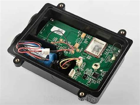
Custom Cable Integration in PCB Assembly
Integrating custom cables into PCB manufacturing workflows requires balancing precision with scalability. When designing cable harnesses, you must account for signal integrity and thermal management while ensuring compatibility with your assembly’s form factor. Leading PCB manufacturing companies leverage modular designs to simplify cable routing, reducing errors during high-volume production.
To minimize PCB manufacturing cost, consider using standardized connectors where possible, but prioritize custom-length wiring for tight spaces. Advanced CAD tools enable virtual prototyping, allowing you to test cable configurations before physical assembly—a critical step for avoiding rework. For PCB manufacturing business models targeting complex systems, hybrid approaches combining automated crimping with manual final adjustments often yield optimal results.
Seamless integration hinges on collaboration between cable suppliers and assembly teams. Specify shielding requirements and bend radius limits early to prevent performance degradation. Transitioning to automated cable management systems? Pair them with inline testing protocols to catch misalignments before final box closure. This proactive approach not only accelerates timelines but also aligns with broader strategies for optimizing PCB manufacturing efficiency across multi-stage builds.
System Testing for Reliable Box Builds
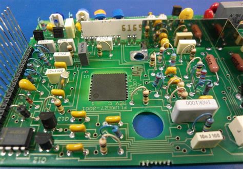
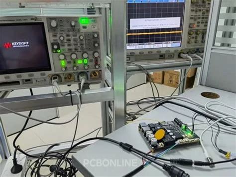
When assembling complex electronics, rigorous system testing ensures your PCB box build meets performance standards and operational safety. Functional validation begins by simulating real-world conditions to verify power distribution, signal integrity, and thermal management. For pcb manufacturing companies, integrating automated test protocols reduces human error while accelerating diagnostics—critical for managing pcb manufacturing cost without compromising quality.
Advanced environmental stress screening (ESS) exposes assemblies to extreme temperatures, vibrations, and humidity, identifying weaknesses in solder joints or component placements early. Pairing these tests with in-circuit checks guarantees every custom cable, connector, and wire harness functions cohesively within the final product. By aligning testing phases with pcb manufacturing business timelines, you avoid costly rework and delays.
Automated optical inspection (AOI) and boundary-scan tools further enhance reliability, especially for high-density boards. These methods validate not just individual parts but how subsystems interact—a necessity for maintaining efficiency in pcb manufacturing. Whether you’re scaling production or refining prototypes, prioritizing end-to-end verification creates robust box builds that withstand long-term use while keeping assembly workflows predictable and cost-effective.
Automated Workflows for Precision Assembly
Implementing automated workflows in pcb manufacturing transforms how you achieve precision in box build assembly. By integrating robotic placement systems and AI-driven inspection tools, repeatability becomes inherent to your production line—critical when handling intricate wire harnesses or custom cables. Leading pcb manufacturing companies now deploy automated optical inspection (AOI) to detect micron-level defects, reducing human error by over 70%. These systems synchronize with enterprise resource planning (ERP) software, allowing real-time adjustments to pcb manufacturing cost variables like material usage or labor allocation.
For complex assemblies, adaptive automation ensures flexible handling of mixed-technology boards, from surface-mount components to through-hole connectors. This approach not only accelerates throughput but also maintains consistency across high-volume orders—a key advantage in competitive pcb manufacturing business environments. By streamlining tasks such as screwdriving or connector mating, automated workflows free engineers to focus on system-level testing protocols. The result? A seamless bridge between assembly accuracy and scalable production, empowering you to meet evolving industry standards without compromising margins.
Cost-Effective Box Build Strategies
Achieving cost efficiency in PCB box build assembly requires balancing quality with smart resource allocation. Start by optimizing design-for-manufacturability (DFM) principles to minimize material waste and reduce PCB manufacturing costs. Work closely with PCB manufacturing companies to standardize component specifications, leveraging bulk purchasing power for connectors, enclosures, and custom cables. Automated wire harness assembly not only accelerates production but also lowers labor expenses, ensuring consistency across high-volume orders.
Consider modular designs that allow reusable subassemblies, cutting downtime between product iterations. Partnering with experienced PCB manufacturing business providers grants access to advanced testing protocols, preventing costly rework by catching defects early. For low-to-mid volume projects, hybrid workflows combining manual precision with robotic automation strike a balance between flexibility and scalability.
Finally, analyze lifecycle costs—not just upfront expenses. Investing in durable materials or energy-efficient components might raise initial PCB manufacturing outlays but reduces long-term operational costs. By aligning your strategy with suppliers’ technical expertise, you can streamline workflows while maintaining competitive pricing for complex electronics.
Complex Electronics Assembly Solutions
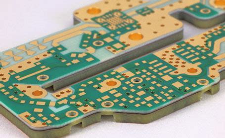
When dealing with intricate electronic systems, integrating PCB manufacturing expertise with multi-layered assembly processes becomes critical. Modern high-density interconnect (HDI) designs and mixed-technology boards demand precision alignment between components, cabling, and enclosures. Leading PCB manufacturing companies now employ robotic placement systems paired with automated optical inspection (AOI) to ensure micron-level accuracy, even when handling miniature connectors or flexible circuits.
A key challenge lies in balancing PCB manufacturing cost with performance requirements. By adopting modular assembly strategies—such as pre-tested subassemblies or standardized wire harness configurations—you reduce rework risks while accelerating time-to-market. Advanced thermal management techniques, including conformal coating and heat-dissipating enclosures, further enhance reliability in mission-critical applications.
For businesses scaling their PCB manufacturing business, cross-functional collaboration between design engineers and production teams is essential. Real-time data sharing through digital twin simulations allows proactive identification of interference points between PCBs, cables, and mechanical housings. This approach not only streamlines workflows but also minimizes material waste—a decisive factor in maintaining competitiveness for complex builds requiring 20+ layer boards or hybrid rigid-flex architectures.
Streamlining Manufacturing with Box Builds
Implementing PCB box build assembly into your production line creates a seamless bridge between board-level fabrication and final product integration. By consolidating PCB manufacturing processes with enclosure assembly, you eliminate redundant handling steps that often create bottlenecks in traditional workflows. Leading PCB manufacturing companies now prioritize system-level integration from the outset, embedding cable harnesses, power supplies, and UI components during the initial build phase rather than as afterthoughts.
This approach directly addresses PCB manufacturing cost challenges by minimizing rework cycles and reducing inventory overhead. Automated alignment systems ensure connectors mate precisely with board interfaces, while modular designs allow rapid reconfiguration for different product variants—critical for maintaining agility in the PCB manufacturing business. You’ll notice improvements in throughput consistency, as testing protocols validate both individual boards and fully assembled units in a single pass.
To maximize efficiency, adopt standardized work instructions that synchronize mechanical assembly with electrical verification. This eliminates guesswork for technicians and accelerates onboarding for new production lines. When paired with predictive maintenance schedules for tooling equipment, your box build strategy becomes a self-reinforcing engine for scalable, error-resistant manufacturing.
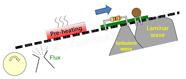
Advanced Wire Harness Assembly Techniques
When integrating wire harnesses into PCB manufacturing, precision and scalability become critical. Modern assembly relies on automated crimping and routing systems to ensure consistent connections, reducing human error while accelerating production timelines. For PCB manufacturing companies, adopting laser-guided placement tools ensures wires align perfectly with board terminals, minimizing signal interference in high-density environments.
A key challenge lies in balancing pcb manufacturing cost with quality. Using modular harness designs allows you to reuse standardized components across projects, cutting material waste and assembly time. Additionally, adaptive testing protocols validate each harness’s electrical continuity before integration, preventing costly rework during final box builds.
To optimize workflows, consider pairing harness assembly with pcb manufacturing business analytics. Real-time monitoring of tension and alignment during wire routing helps identify bottlenecks, enabling proactive adjustments. For complex configurations, employing shielded cables and custom connectors enhances EMI resistance—a necessity for aerospace or medical electronics.
By aligning these techniques with your broader PCB manufacturing strategy, you create seamless transitions between harness integration and system testing. This not only elevates product reliability but also positions your operations to handle evolving industry demands without sacrificing efficiency.
Optimizing PCB Box Build Efficiency
To maximize efficiency in PCB box build processes, you must align design intent with production realities. Start by evaluating design complexity early—collaborate with PCB manufacturing companies to identify potential bottlenecks in component placement or cable routing. Implementing automated workflows reduces manual errors and accelerates throughput, particularly when handling high-volume orders. Consider PCB manufacturing cost drivers like material selection; opting for standardized connectors instead of custom parts can trim expenses without sacrificing quality.
Integrate design-for-manufacturability (DFM) principles to simplify assembly steps—this approach minimizes rework and streamlines validation phases. For PCB manufacturing business scalability, leverage volume discounts on common components while maintaining a diversified supplier network to mitigate supply chain risks. Real-time monitoring systems provide visibility into production metrics, enabling quick adjustments to maintain cycle time targets. Pair these strategies with rigorous functional testing protocols to catch defects before final integration, ensuring reliability without compromising delivery schedules. By balancing technical precision with cost-conscious decision-making, you create a responsive PCB manufacturing ecosystem capable of adapting to evolving product demands.
Conclusion
In today’s competitive landscape, optimizing PCB manufacturing processes requires a strategic balance of innovation and cost efficiency. For PCB manufacturing companies, mastering advanced box build assembly techniques ensures seamless integration of custom cables, wire harnesses, and rigorous system testing—key elements for delivering reliable, high-performance electronics. By focusing on PCB manufacturing cost reduction through automated workflows and precision assembly, you can eliminate bottlenecks while maintaining quality standards.
Implementing these strategies not only streamlines production but also strengthens your PCB manufacturing business by addressing complex assembly challenges. Whether refining wire routing or enhancing testing protocols, every decision should prioritize scalability and repeatability. Lean methodologies paired with advanced automation tools empower you to meet evolving market demands without compromising on speed or accuracy.
Ultimately, the success of your box build projects hinges on aligning technical expertise with operational agility. By leveraging modern techniques, you position your operations to thrive in an industry where precision, efficiency, and cost-effectiveness define long-term competitiveness.
FAQs
How does custom cable integration affect pcb manufacturing costs?
By standardizing connectors and using modular designs, you can reduce material waste and labor hours. Leading pcb manufacturing companies often leverage automated cable routing to minimize errors that drive up expenses.
What quality checks ensure reliable box builds in high-volume production?
Comprehensive system testing—including in-circuit and functional tests—validates every assembly layer. Partnering with certified pcb manufacturing businesses ensures adherence to IPC standards, reducing post-deployment failures.
Can automation lower pcb manufacturing costs for complex builds?
Yes. Robotic soldering and AI-driven inspection systems optimize precision while cutting rework rates. Many pcb manufacturing providers now offer scalable automation packages tailored to mid-sized batches.
How do you balance cost and quality when selecting a pcb manufacturing company?
Evaluate their expertise in design-for-manufacturing (DFM) feedback and supply chain transparency. Tier-1 suppliers often provide cost-breakdown analyses, helping you identify savings without compromising reliability.
What trends are reshaping the pcb manufacturing business for box builds?
Demand for IoT-compatible enclosures and edge-computing integrations is rising. Forward-thinking manufacturers now combine thermal management solutions with lightweight materials to meet evolving industry needs.
Ready to Elevate Your PCB Box Build Strategy?
For tailored solutions that align with your pcb manufacturing goals, please click here to connect with experts specializing in advanced assembly techniques.