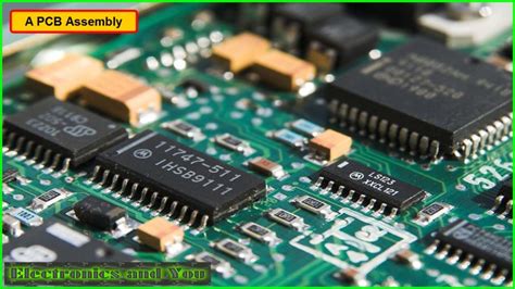
Advanced pcb design
High-Speed Signal Integrity in Advanced PCB Design
In the realm of advanced printed circuit board (PCB) design, high-speed signal integrity has emerged as a critical consideration. As electronic devices become increasingly sophisticated, the demand for faster data transmission rates has surged, necessitating meticulous attention to signal integrity.
Ensuring high-speed signal integrity involves a comprehensive understanding of various factors that can affect signal quality, including impedance control, crosstalk, and electromagnetic interference (EMI).
To begin with, impedance control is paramount in high-speed PCB design.
Impedance mismatches can lead to signal reflections, which degrade the quality of the signal and can cause data errors. Designers must carefully calculate and control the impedance of traces to match the impedance of the source and load. This often involves selecting the appropriate materials, such as high-frequency laminates, and precisely controlling the trace width and spacing. Additionally, the use of differential pairs, where two complementary signals are routed together, can help maintain signal integrity by reducing susceptibility to external noise and minimizing signal reflections.
Transitioning to the issue of crosstalk, it is essential to recognize that as signal frequencies increase, the likelihood of crosstalk between adjacent traces also rises.
Crosstalk occurs when a signal in one trace induces an unwanted signal in a neighboring trace, potentially leading to data corruption. To mitigate crosstalk, designers can employ several strategies, such as increasing the spacing between traces, using ground planes to provide a return path for signals, and implementing guard traces. Guard traces, which are grounded traces placed between signal lines, can effectively shield signals from one another and reduce crosstalk.
Moreover, electromagnetic interference (EMI) poses a significant challenge in high-speed PCB design.
EMI can emanate from various sources, including power supplies, clock signals, and external electronic devices, and can interfere with the proper functioning of the PCB. To combat EMI, designers must adopt a holistic approach that encompasses both layout and component selection. Shielding techniques, such as using metal enclosures or ground planes, can help contain EMI and prevent it from affecting sensitive components. Additionally, selecting components with low electromagnetic emissions and designing power distribution networks with proper decoupling capacitors can further enhance EMI performance.
Furthermore, the role of simulation and modeling cannot be overstated in ensuring high-speed signal integrity.
Advanced simulation tools allow designers to predict and analyze the behavior of high-speed signals before physical prototyping. By simulating signal propagation, impedance, crosstalk, and EMI, designers can identify potential issues and make necessary adjustments early in the design process. This not only saves time and resources but also increases the likelihood of achieving optimal signal integrity in the final product.
In addition to simulation, adhering to best practices in PCB layout is crucial.
For instance, maintaining consistent trace widths and avoiding sharp bends can minimize impedance discontinuities. Routing high-speed signals on inner layers, sandwiched between ground planes, can provide better shielding and reduce EMI. Moreover, ensuring proper grounding and power distribution is essential for maintaining signal integrity. A well-designed ground plane can provide a low-impedance return path for signals, reducing noise and improving overall performance.
In conclusion, high-speed signal integrity in advanced PCB design is a multifaceted challenge that requires a thorough understanding of impedance control, crosstalk mitigation, and EMI management. By employing a combination of careful material selection, strategic layout techniques, and advanced simulation tools, designers can effectively address these challenges and ensure the reliable performance of high-speed electronic devices. As technology continues to evolve, the importance of maintaining high-speed signal integrity will only grow, underscoring the need for ongoing innovation and expertise in PCB design.
Thermal Management Techniques for Complex PCBs
Thermal management is a critical aspect of advanced PCB design, particularly as electronic devices become more powerful and compact. Effective thermal management techniques are essential to ensure the reliability, performance, and longevity of complex printed circuit boards (PCBs). As electronic components generate heat during operation, it is imperative to dissipate this heat efficiently to prevent overheating and potential failure.
One of the primary techniques for thermal management in PCBs is the use of thermal vias.
These are small, plated holes that connect the different layers of a PCB, allowing heat to transfer from the surface-mounted components to the inner layers and ultimately to the heat sinks or other cooling mechanisms. By providing a direct path for heat to escape, thermal vias help to maintain lower temperatures on the surface of the PCB, thereby protecting sensitive components from thermal stress.
In addition to thermal vias, the incorporation of heat sinks is another effective method for managing heat in complex PCBs.
Heat sinks are typically made of materials with high thermal conductivity, such as aluminum or copper, and are designed to absorb and dissipate heat away from critical components. By increasing the surface area available for heat dissipation, heat sinks can significantly reduce the temperature of the components they are attached to. This is particularly important for high-power devices, where excessive heat generation can lead to performance degradation or even catastrophic failure.
Furthermore, the use of thermal interface materials (TIMs) is crucial in enhancing the thermal conductivity between components and heat sinks.
TIMs, such as thermal pads, thermal grease, or phase-change materials, fill the microscopic air gaps that naturally occur between surfaces, thereby improving the efficiency of heat transfer. By ensuring a more uniform and effective thermal connection, TIMs play a vital role in maintaining optimal operating temperatures for electronic components.
Another advanced technique for thermal management in PCBs is the implementation of thermal planes.
These are dedicated layers within the PCB that are specifically designed to spread and dissipate heat. Typically made of copper, thermal planes can be strategically placed near heat-generating components to facilitate the efficient transfer of heat away from these areas. By distributing heat more evenly across the PCB, thermal planes help to prevent localized hotspots and reduce the overall thermal resistance of the board.
Moreover, the design of the PCB layout itself can significantly impact thermal management.
For instance, placing high-power components in areas with better airflow or near the edges of the PCB can enhance heat dissipation. Additionally, optimizing the trace width and spacing can reduce the thermal resistance of the conductive paths, thereby improving heat transfer. Careful consideration of component placement and routing can thus play a pivotal role in managing the thermal performance of complex PCBs.
Lastly, active cooling solutions, such as fans or liquid cooling systems, can be employed for PCBs that require more aggressive thermal management.
While these solutions are typically more complex and costly, they can provide substantial cooling capabilities for high-performance applications. By actively removing heat from the PCB, these systems can maintain lower operating temperatures and ensure the reliable operation of the electronic device.
In conclusion, effective thermal management is essential for the successful design and operation of advanced PCBs. By employing a combination of techniques such as thermal vias, heat sinks, thermal interface materials, thermal planes, optimized PCB layout, and active cooling solutions, designers can ensure that their PCBs operate within safe temperature ranges. This not only enhances the performance and reliability of the electronic device but also extends its operational lifespan, making thermal management a critical consideration in modern PCB design.
Advanced Layer Stackup Strategies for Multilayer PCBs
In the realm of advanced PCB design, the strategic implementation of multilayer stackups is paramount to achieving optimal performance and reliability. As electronic devices become increasingly complex, the demand for sophisticated multilayer PCBs has surged, necessitating a deeper understanding of advanced layer stackup strategies. These strategies are essential for managing signal integrity, power distribution, and thermal performance, all of which are critical to the functionality of modern electronic systems.
To begin with, the fundamental concept of a multilayer PCB involves the stacking of multiple layers of conductive and insulating materials.
This configuration allows for a higher density of components and interconnections, which is indispensable for contemporary electronic devices. The primary objective of an advanced layer stackup strategy is to minimize electromagnetic interference (EMI) and crosstalk while ensuring robust power delivery and thermal management. Achieving this balance requires meticulous planning and a thorough understanding of the electrical and thermal properties of the materials involved.
One of the key considerations in advanced layer stackup design is the arrangement of signal and power layers.
Typically, signal layers are interspersed with ground and power planes to provide effective shielding and reduce EMI. For instance, placing a ground plane adjacent to a signal layer can significantly diminish the loop area, thereby minimizing radiated emissions. Additionally, the use of multiple ground planes can further enhance signal integrity by providing a low-impedance return path for high-frequency signals. This approach is particularly beneficial in high-speed digital circuits where signal integrity is paramount.
Moreover, the selection of dielectric materials plays a crucial role in the performance of multilayer PCBs.
Dielectric materials with low permittivity and low loss tangent are preferred for high-frequency applications as they reduce signal attenuation and dispersion. Furthermore, the thickness of the dielectric layers must be carefully controlled to maintain the desired impedance levels. Impedance control is vital for ensuring signal integrity, especially in high-speed and high-frequency circuits. Advanced simulation tools can aid in predicting the electrical behavior of the stackup, allowing designers to make informed decisions about material selection and layer thickness.
Thermal management is another critical aspect of advanced layer stackup strategies.
As electronic devices continue to shrink in size while increasing in power density, effective heat dissipation becomes a significant challenge. Incorporating thermal vias and dedicated thermal layers within the stackup can facilitate efficient heat transfer away from critical components. Additionally, the use of materials with high thermal conductivity, such as metal cores or embedded heat spreaders, can further enhance thermal performance. Proper thermal management not only ensures the longevity of the components but also maintains the overall reliability of the PCB.
Power distribution is equally important in multilayer PCB design.
A well-designed power distribution network (PDN) ensures stable voltage levels across the board, minimizing voltage drops and noise. This can be achieved by strategically placing power and ground planes to create a low-impedance path for current flow. Decoupling capacitors should be placed close to the power pins of integrated circuits to filter out high-frequency noise and provide a stable power supply. Advanced PDN analysis tools can help designers optimize the placement and routing of power and ground planes to achieve the desired performance.
In conclusion, advanced layer stackup strategies for multilayer PCBs are essential for meeting the demands of modern electronic systems.
By carefully considering the arrangement of signal and power layers, selecting appropriate dielectric materials, managing thermal performance, and ensuring robust power distribution, designers can create PCBs that deliver superior performance and reliability. As technology continues to evolve, the importance of advanced layer stackup strategies will only grow, making it a critical area of focus for PCB designers.
Design for Manufacturability (DFM) in High-Density PCB Layouts
Design for Manufacturability (DFM) is a critical consideration in the development of high-density printed circuit board (PCB) layouts. As electronic devices continue to shrink in size while increasing in functionality, the complexity of PCB designs has escalated. This necessitates a meticulous approach to ensure that the designs are not only functional but also manufacturable at scale. The integration of DFM principles into high-density PCB layouts is essential to mitigate potential production issues, reduce costs, and enhance overall product reliability.
One of the primary challenges in high-density PCB design is managing the limited space available for routing traces and placing components.
To address this, designers must employ advanced techniques such as microvias, buried vias, and blind vias. These methods allow for more efficient use of the PCB’s layers, enabling higher component density without compromising signal integrity. However, the use of such techniques must be carefully balanced with the capabilities of the manufacturing process. For instance, the aspect ratio of vias and the precision required for drilling and plating must align with the manufacturer’s capabilities to avoid defects and ensure yield.
Moreover, the selection of materials plays a pivotal role in the manufacturability of high-density PCBs.
The choice of substrate material, copper thickness, and solder mask type can significantly impact the performance and reliability of the final product. High-frequency applications, for example, may require low-loss materials to maintain signal integrity. Additionally, thermal management becomes increasingly important as component density rises. Effective heat dissipation strategies, such as the use of thermal vias and heat sinks, must be incorporated into the design to prevent overheating and ensure long-term reliability.
Transitioning from design to production, it is crucial to consider the assembly process.
Surface mount technology (SMT) is commonly used for high-density PCBs due to its ability to place small components with high precision. However, the design must accommodate the limitations of SMT equipment, such as minimum component spacing and placement accuracy. Furthermore, the soldering process must be optimized to prevent issues such as tombstoning, where components lift off the PCB during reflow soldering. This can be achieved by ensuring uniform pad sizes and proper stencil design for solder paste application.
Testing and inspection are also integral to the DFM process.
High-density PCBs often require advanced testing methods, such as automated optical inspection (AOI) and X-ray inspection, to detect defects that are not visible to the naked eye. Designing test points and incorporating built-in self-test (BIST) features can facilitate thorough testing and improve fault detection. Additionally, considering the ease of rework and repair during the design phase can save significant time and cost in the event of defects.
In conclusion, the successful implementation of DFM principles in high-density PCB layouts requires a holistic approach that encompasses design, material selection, assembly, and testing.
By carefully considering the manufacturability aspects throughout the design process, engineers can create high-density PCBs that are not only functional but also reliable and cost-effective to produce. This approach not only enhances the quality of the final product but also ensures a smoother transition from design to mass production, ultimately contributing to the success of electronic devices in an increasingly competitive market.High-Speed Signal Integrity in Advanced PCB Design
In the realm of advanced printed circuit board (PCB) design, high-speed signal integrity has emerged as a critical consideration.
As electronic devices become increasingly sophisticated, the demand for faster data transmission rates has surged, necessitating meticulous attention to signal integrity. Ensuring high-speed signal integrity involves a comprehensive understanding of various factors that can affect signal quality, including impedance control, crosstalk, and electromagnetic interference (EMI).
To begin with, impedance control is paramount in high-speed PCB design.
Impedance mismatches can lead to signal reflections, which degrade the quality of the signal and can cause data errors. Designers must carefully calculate and control the impedance of traces to match the impedance of the source and load. This often involves selecting the appropriate materials, such as high-frequency laminates, and precisely controlling the trace width and spacing. Additionally, the use of differential pairs, where two complementary signals are routed together, can help maintain signal integrity by reducing susceptibility to external noise and minimizing signal reflections.
Transitioning to the issue of crosstalk, it is essential to recognize that as signal frequencies increase, the likelihood of crosstalk between adjacent traces also rises.
Crosstalk occurs when a signal in one trace induces an unwanted signal in a neighboring trace, potentially leading to data corruption. To mitigate crosstalk, designers can employ several strategies, such as increasing the spacing between traces, using ground planes to provide a return path for signals, and implementing guard traces. Guard traces, which are grounded traces placed between signal lines, can effectively shield signals from one another and reduce crosstalk.
Moreover, electromagnetic interference (EMI) poses a significant challenge in high-speed PCB design.
EMI can emanate from various sources, including power supplies, clock signals, and external electronic devices, and can interfere with the proper functioning of the PCB. To combat EMI, designers must adopt a holistic approach that encompasses both layout and component selection. Shielding techniques, such as using metal enclosures or ground planes, can help contain EMI and prevent it from affecting sensitive components. Additionally, selecting components with low electromagnetic emissions and designing power distribution networks with proper decoupling capacitors can further enhance EMI performance.
Furthermore, the role of simulation and modeling cannot be overstated in ensuring high-speed signal integrity.
Advanced simulation tools allow designers to predict and analyze the behavior of high-speed signals before physical prototyping. By simulating signal propagation, impedance, crosstalk, and EMI, designers can identify potential issues and make necessary adjustments early in the design process. This not only saves time and resources but also increases the likelihood of achieving optimal signal integrity in the final product.
In addition to simulation, adhering to best practices in PCB layout is crucial.
For instance, maintaining consistent trace widths and avoiding sharp bends can minimize impedance discontinuities. Routing high-speed signals on inner layers, sandwiched between ground planes, can provide better shielding and reduce EMI. Moreover, ensuring proper grounding and power distribution is essential for maintaining signal integrity. A well-designed ground plane can provide a low-impedance return path for signals, reducing noise and improving overall performance.
In conclusion, high-speed signal integrity in advanced PCB design is a multifaceted challenge that requires a thorough understanding of impedance control, crosstalk mitigation, and EMI management. By employing a combination of careful material selection, strategic layout techniques, and advanced simulation tools, designers can effectively address these challenges and ensure the reliable performance of high-speed electronic devices. As technology continues to evolve, the importance of maintaining high-speed signal integrity will only grow, underscoring the need for ongoing innovation and expertise in PCB design.
Thermal Management Techniques for Complex PCBs
Thermal management is a critical aspect of advanced PCB design, particularly as electronic devices become more powerful and compact. Effective thermal management techniques are essential to ensure the reliability, performance, and longevity of complex printed circuit boards (PCBs). As electronic components generate heat during operation, it is imperative to dissipate this heat efficiently to prevent overheating and potential failure.
One of the primary techniques for thermal management in PCBs is the use of thermal vias.
These are small, plated holes that connect the different layers of a PCB, allowing heat to transfer from the surface-mounted components to the inner layers and ultimately to the heat sinks or other cooling mechanisms. By providing a direct path for heat to escape, thermal vias help to maintain lower temperatures on the surface of the PCB, thereby protecting sensitive components from thermal stress.
In addition to thermal vias, the incorporation of heat sinks is another effective method for managing heat in complex PCBs.
Heat sinks are typically made of materials with high thermal conductivity, such as aluminum or copper, and are designed to absorb and dissipate heat away from critical components. By increasing the surface area available for heat dissipation, heat sinks can significantly reduce the temperature of the components they are attached to. This is particularly important for high-power devices, where excessive heat generation can lead to performance degradation or even catastrophic failure.
Furthermore, the use of thermal interface materials (TIMs) is crucial in enhancing the thermal conductivity between components and heat sinks.
TIMs, such as thermal pads, thermal grease, or phase-change materials, fill the microscopic air gaps that naturally occur between surfaces, thereby improving the efficiency of heat transfer. By ensuring a more uniform and effective thermal connection, TIMs play a vital role in maintaining optimal operating temperatures for electronic components.
Another advanced technique for thermal management in PCBs is the implementation of thermal planes.
These are dedicated layers within the PCB that are specifically designed to spread and dissipate heat. Typically made of copper, thermal planes can be strategically placed near heat-generating components to facilitate the efficient transfer of heat away from these areas. By distributing heat more evenly across the PCB, thermal planes help to prevent localized hotspots and reduce the overall thermal resistance of the board.
Moreover, the design of the PCB layout itself can significantly impact thermal management.
For instance, placing high-power components in areas with better airflow or near the edges of the PCB can enhance heat dissipation. Additionally, optimizing the trace width and spacing can reduce the thermal resistance of the conductive paths, thereby improving heat transfer. Careful consideration of component placement and routing can thus play a pivotal role in managing the thermal performance of complex PCBs.
Lastly, active cooling solutions, such as fans or liquid cooling systems, can be employed for PCBs that require more aggressive thermal management.
While these solutions are typically more complex and costly, they can provide substantial cooling capabilities for high-performance applications. By actively removing heat from the PCB, these systems can maintain lower operating temperatures and ensure the reliable operation of the electronic device.
In conclusion, effective thermal management is essential for the successful design and operation of advanced PCBs. By employing a combination of techniques such as thermal vias, heat sinks, thermal interface materials, thermal planes, optimized PCB layout, and active cooling solutions, designers can ensure that their PCBs operate within safe temperature ranges. This not only enhances the performance and reliability of the electronic device but also extends its operational lifespan, making thermal management a critical consideration in modern PCB design.
Advanced Layer Stackup Strategies for Multilayer PCBs
In the realm of advanced PCB design, the strategic implementation of multilayer stackups is paramount to achieving optimal performance and reliability. As electronic devices become increasingly complex, the demand for sophisticated multilayer PCBs has surged, necessitating a deeper understanding of advanced layer stackup strategies. These strategies are essential for managing signal integrity, power distribution, and thermal performance, all of which are critical to the functionality of modern electronic systems.
To begin with, the fundamental concept of a multilayer PCB involves the stacking of multiple layers of conductive and insulating materials.
This configuration allows for a higher density of components and interconnections, which is indispensable for contemporary electronic devices. The primary objective of an advanced layer stackup strategy is to minimize electromagnetic interference (EMI) and crosstalk while ensuring robust power delivery and thermal management. Achieving this balance requires meticulous planning and a thorough understanding of the electrical and thermal properties of the materials involved.
One of the key considerations in advanced layer stackup design is the arrangement of signal and power layers.
Typically, signal layers are interspersed with ground and power planes to provide effective shielding and reduce EMI. For instance, placing a ground plane adjacent to a signal layer can significantly diminish the loop area, thereby minimizing radiated emissions. Additionally, the use of multiple ground planes can further enhance signal integrity by providing a low-impedance return path for high-frequency signals. This approach is particularly beneficial in high-speed digital circuits where signal integrity is paramount.
Moreover, the selection of dielectric materials plays a crucial role in the performance of multilayer PCBs.
Dielectric materials with low permittivity and low loss tangent are preferred for high-frequency applications as they reduce signal attenuation and dispersion. Furthermore, the thickness of the dielectric layers must be carefully controlled to maintain the desired impedance levels. Impedance control is vital for ensuring signal integrity, especially in high-speed and high-frequency circuits. Advanced simulation tools can aid in predicting the electrical behavior of the stackup, allowing designers to make informed decisions about material selection and layer thickness.
Thermal management is another critical aspect of advanced layer stackup strategies.
As electronic devices continue to shrink in size while increasing in power density, effective heat dissipation becomes a significant challenge. Incorporating thermal vias and dedicated thermal layers within the stackup can facilitate efficient heat transfer away from critical components. Additionally, the use of materials with high thermal conductivity, such as metal cores or embedded heat spreaders, can further enhance thermal performance. Proper thermal management not only ensures the longevity of the components but also maintains the overall reliability of the PCB.
Power distribution is equally important in multilayer PCB design.
A well-designed power distribution network (PDN) ensures stable voltage levels across the board, minimizing voltage drops and noise. This can be achieved by strategically placing power and ground planes to create a low-impedance path for current flow. Decoupling capacitors should be placed close to the power pins of integrated circuits to filter out high-frequency noise and provide a stable power supply. Advanced PDN analysis tools can help designers optimize the placement and routing of power and ground planes to achieve the desired performance.
In conclusion, advanced layer stackup strategies for multilayer PCBs are essential for meeting the demands of modern electronic systems. By carefully considering the arrangement of signal and power layers, selecting appropriate dielectric materials, managing thermal performance, and ensuring robust power distribution, designers can create PCBs that deliver superior performance and reliability. As technology continues to evolve, the importance of advanced layer stackup strategies will only grow, making it a critical area of focus for PCB designers.
Design for Manufacturability (DFM) in High-Density PCB Layouts
Design for Manufacturability (DFM) is a critical consideration in the development of high-density printed circuit board (PCB) layouts. As electronic devices continue to shrink in size while increasing in functionality, the complexity of PCB designs has escalated. This necessitates a meticulous approach to ensure that the designs are not only functional but also manufacturable at scale. The integration of DFM principles into high-density PCB layouts is essential to mitigate potential production issues, reduce costs, and enhance overall product reliability.
One of the primary challenges in high-density PCB design is managing the limited space available for routing traces and placing components.
To address this, designers must employ advanced techniques such as microvias, buried vias, and blind vias. These methods allow for more efficient use of the PCB’s layers, enabling higher component density without compromising signal integrity. However, the use of such techniques must be carefully balanced with the capabilities of the manufacturing process. For instance, the aspect ratio of vias and the precision required for drilling and plating must align with the manufacturer’s capabilities to avoid defects and ensure yield.
Moreover, the selection of materials plays a pivotal role in the manufacturability of high-density PCBs.
The choice of substrate material, copper thickness, and solder mask type can significantly impact the performance and reliability of the final product. High-frequency applications, for example, may require low-loss materials to maintain signal integrity. Additionally, thermal management becomes increasingly important as component density rises. Effective heat dissipation strategies, such as the use of thermal vias and heat sinks, must be incorporated into the design to prevent overheating and ensure long-term reliability.
Transitioning from design to production, it is crucial to consider the assembly process.
Surface mount technology (SMT) is commonly used for high-density PCBs due to its ability to place small components with high precision. However, the design must accommodate the limitations of SMT equipment, such as minimum component spacing and placement accuracy. Furthermore, the soldering process must be optimized to prevent issues such as tombstoning, where components lift off the PCB during reflow soldering. This can be achieved by ensuring uniform pad sizes and proper stencil design for solder paste application.
Testing and inspection are also integral to the DFM process.
High-density PCBs often require advanced testing methods, such as automated optical inspection (AOI) and X-ray inspection, to detect defects that are not visible to the naked eye. Designing test points and incorporating built-in self-test (BIST) features can facilitate thorough testing and improve fault detection. Additionally, considering the ease of rework and repair during the design phase can save significant time and cost in the event of defects.
In conclusion, the successful implementation of DFM principles in high-density PCB layouts requires a holistic approach that encompasses design, material selection, assembly, and testing. By carefully considering the manufacturability aspects throughout the design process, engineers can create high-density PCBs that are not only functional but also reliable and cost-effective to produce. This approach not only enhances the quality of the final product but also ensures a smoother transition from design to mass production, ultimately contributing to the success of electronic devices in an increasingly competitive market.


