Advanced PCB Design: PCB Thermal Design Optimization
For hardware engineers, the level of PCB design directly affects the performance and stability of electronic products. In the previous series of articles, we explored many key points of PCB design. This article will continue to go deeper and focus on some aspects that are easy to overlook but crucial, helping hardware engineers to further improve their PCB design skills.
1.Layout Design
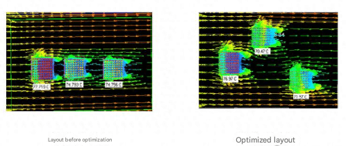
① Are high-power heating components placed near the edge of the PCB or vents, which are easy to dissipate heat? CFD (Computational Fluid Dynamics) simulation software can be used to analyze the air flow and heat dissipation effects of different placement positions to determine the best position.
② Is there enough spacing between heating components to avoid heat accumulation? According to the results of thermal simulation analysis, the appropriate spacing value can be set to ensure effective heat dissipation. Heating devices should be arranged as dispersed as possible to make the heat consumption on the surface of the single board uniform, which is conducive to heat dissipation.
③ Are sensitive components away from heating components? Through heat-affected zone analysis, determine the safe distance between sensitive components and heating components. Do not place heat-sensitive devices or devices with high power consumption close to each other, and keep heat-sensitive devices away from high-temperature heating devices.
- Common heat-sensitive devices include crystal oscillators, memory, CPU, etc. Heat-sensitive components should be placed in the coldest area.
- For natural convection cooling equipment, if the shell is sealed, heat-sensitive devices should be placed at the bottom and other components should be placed at the top; if the shell is not sealed, heat-sensitive devices should be placed at the entrance of cold air.
- For forced convection cooling equipment, heat-sensitive components can be placed at the entrance of air flow.
④ Design the device layout based on the characteristics of flow velocity distribution in the board.
- In a specific air duct, the surface flow velocity of a single board with a large area is inevitably uneven. The area with a large flow velocity is conducive to heat dissipation. Fully considering this factor for layout design will enable the single board to obtain a better heat dissipation design.
⑤ For devices that dissipate heat through PWB, since they rely on the overall area of PWB to dissipate heat, even if the device is in an area with low local wind speed, there will not necessarily be a heat dissipation problem. On the basis of sufficient thermal analysis and verification, it is not necessary to unilaterally require uniform wind speed on the surface of the single board.
⑥ When a series of devices arranged along the direction of airflow need to be equipped with a heat sink. the devices should be arranged in a staggered manner along the direction of airflow as much as possible, which can reduce the mutual influence between upstream and downstream devices.
- If it is not possible to arrange them in a staggered manner, it is also necessary to avoid placing tall components (structural parts, etc.) above high-heat generating components.
⑦ For devices with heat sinks installed, air will flow around the device when it flows through it, which will enhance the heat transfer coefficient of the devices on both sides of the device; the heat transfer coefficient of the devices downstream of the device may be enhanced or weakened, so special attention should be paid to the devices blocked by the heat sink.
⑧ Pay attention to the problem of uniform wind resistance of the single board: the devices on the single board should be arranged as dispersed and evenly as possible to avoid leaving a large airspace along the direction of the wind duct, which will affect the overall heat dissipation effect of the components on the single board.
When electronic equipment is running, chips and other components will generate heat. If the heat cannot be effectively dissipated, the performance of the components will be reduced or even damaged. When laying out, components with high heat generation (such as power chips, high-power resistors, etc.) should be placed in a position that is conducive to heat dissipation, such as near the air inlet or in a position with high wind speed.
- At the same time, avoid placing temperature-sensitive components (such as crystal oscillators and certain sensors) near heating components to prevent their performance from being affected by temperature.
For example, when designing an industrial control board, the power MOSFET is concentrated on the edge of the PCB, and a large area of heat dissipation copper foil is set below it. At the same time, vias are added to the copper foil to form “thermal vias”, which effectively enhances the heat dissipation effect. In this way, the temperature of key components of the control board can still be kept within a reasonable range under long-term high-load operation, ensuring the stability of the system. In addition, a stable temperature environment also has a positive impact on signal integrity.
Overheating may cause component parameter drift, which in turn affects the accuracy and stability of signal transmission. Good thermal management can provide the basic conditions for stable signal transmission.
2.Use appropriate heat dissipation design for devices with different packages
A good single-board heat dissipation solution must be designed according to the heat dissipation characteristics of the device! THD devices have a small number of pins, and the package is not close to the single board after welding, and the thermal correlation with the single board is very small. The heat of this type of device is dissipated to the environment through the surface of the device. Therefore, early device heat dissipation research focused on the air flow on the device surface in order to obtain a relatively high device surface convection heat transfer coefficient.
SMD devices have high integration and high heat consumption, and are the focus of heat dissipation.
This type of device has a large number of pins/solder balls, and the package is also close to the single board after welding, establishing a close heat exchange relationship with the single board. The heat dissipation solution must be analyzed from the perspective of the overall heat dissipation of the single board. SMD devices have also appeared in a variety of enhanced heat dissipation packages for heat dissipation needs.
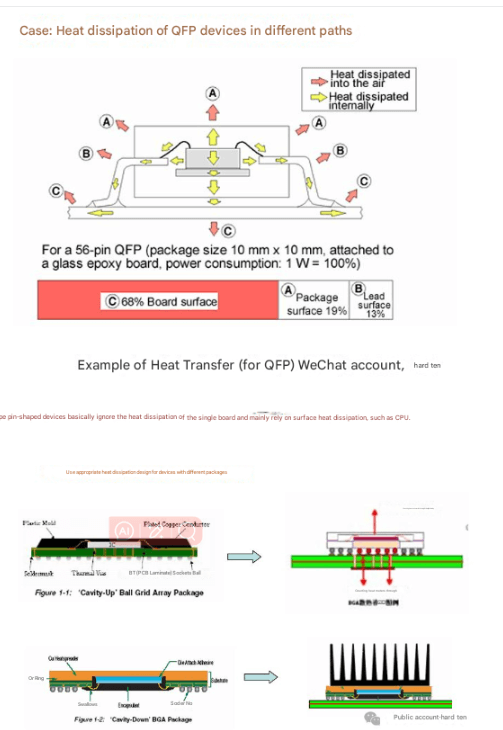
These packages are of various types, but from the perspective of heat dissipation, pin packages and solder ball packages are the most typical. The heat dissipation characteristics of other packages can refer to these two analogies.
PGA-type pin-shaped devices basically ignore single-board heat dissipation and mainly use surface heat dissipation, such as CPUs.
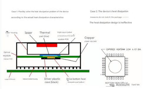
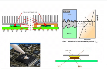
[Design experience] Shared heat sinks need to consider device tolerances and the thickness of thermal conductive silicone.
For the EGPU board, the simulation conclusion of the company’s thermal design shows a relatively high temperature, while the temperature of the Intel heat dissipation simulation model is relatively low when using the same simulation model. After discussing with Intel in the afternoon, the reason is that the thickness of the thermal conductive glue between the CPU and the radiator in the simulation model established by Intel is 0.13mm, while the simulation model used in our current simulation model is 0.3mm.
As a result, the temperature of the CPU in the Intel simulation model is 95 degrees Celsius, while our simulation result is: greater than 116 degrees Celsius. 0.3mm is an empirical value obtained by referring to the tolerance of the two devices, and a reference value with a relatively high probability is selected. Intel believes that if elastic rubber pads are used for screw installation, thermal pads (thicker) are added to the PCH, and thermal conductive glue is added to the CPU, it can ensure that the CPU and the radiator are fully bonded.
- Whether it can reach 0.2mm or 0.13mm requires structural and process confirmation.
- How to achieve a gap of 0.13mm requires Intel to provide a basis, or to provide cases and solutions.
3.PCB auxiliary heat dissipation
For electronic equipment, a certain amount of heat will be generated during operation, which will cause the internal temperature of the equipment to rise rapidly. If the heat is not dissipated in time, the equipment will continue to heat up, the device will fail due to overheating, and the reliability of the electronic equipment will decrease. Therefore, it is very important to perform good heat dissipation treatment on the circuit board.
1.Add heat dissipation copper foil and use large-area power ground copper foil.
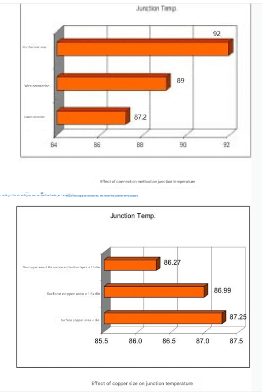
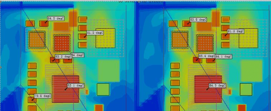
According to the above figure, it can be seen that the larger the area of the copper foil, the lower the junction temperature
According to the above figure, it can be seen that the larger the copper covering area, the lower the junction temperature.
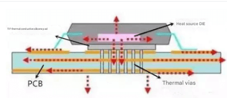
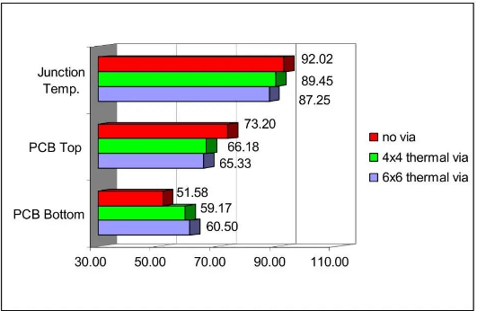
2.Thermal vias
Thermal vias can effectively reduce the junction temperature of the device and improve the uniformity of the temperature in the thickness direction of the single board, which provides the possibility of taking other heat dissipation methods on the back of the PCB. Through simulation, it is found that compared with no thermal vias, the thermal vias with a device thermal power consumption of 2.5W, a spacing of 1mm, and a center design of 6×6 can reduce the junction temperature by about 4.8°C, and the temperature difference between the top and bottom surfaces of the PCB is reduced from the original 21°C to 5°C. After the thermal via array is changed to 4×4, the junction temperature of the device is increased by 2.2°C compared with 6×6, which is worthy of attention.
3.The copper is exposed on the back of the IC to reduce the thermal resistance between the copper skin and the air
In terms of thermal management, although industry standards such as IPC-2221B “General Standard for Printed Board Design” do not specifically specify thermal management in detail, they emphasize the balance between electrical, mechanical and thermal performance in the overall design principles. Engineers should refer to this standard when designing to ensure that thermal management measures do not have a negative impact on other performance of the PCB. For example, the design of large-area heat dissipation copper foil cannot affect the mechanical strength of the PCB, and the setting of thermal vias should consider the impact on other circuits and components.
4.Thermal resistance analysis
Has the overall thermal resistance of the PCB been calculated and analyzed?
Is the thermal resistance of the critical path within an acceptable range?
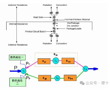
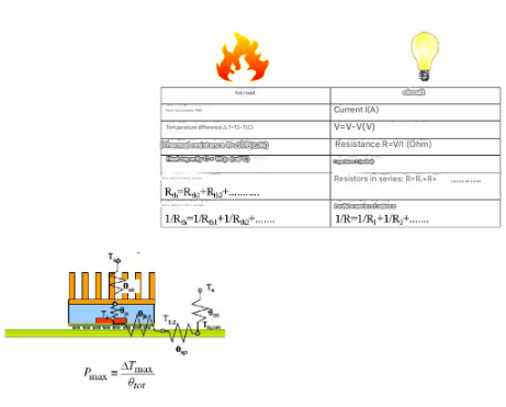
In the process of heat transfer, the temperature difference is the driving force of the process, like the voltage in electricity, and the heat transfer amount is the amount transferred, like the current in electricity.
- Therefore, the denominator in the above formula can be understood as the resistance of the heat conduction process using the concept of resistance in electricity, called thermal resistance, with a unit of ℃/W. Its physical meaning is how many degrees of temperature difference is required to transfer 1W of heat.
- In thermal design, thermal resistance is marked as R or θ. δ/(λA) is the thermal resistance of thermal conduction, and 1/αA is the thermal resistance of convection heat transfer.
- The device data generally provides the device’s Rjc and Rja thermal resistances. Rjc is the device’s junction-to-shell thermal resistance; Rja is the sum of the device’s junction-to-shell thermal resistance and the shell’s convection heat transfer resistance.
- These thermal resistance parameters can be obtained from experimental tests or calculated based on the detailed device’s internal structure. Based on these thermal resistance parameters and the device’s heat dissipation, the device’s junction temperature can be calculated.
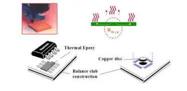
Two nominally contacting solid surfaces actually only contact on some discrete area elements. As shown in the right figure, the gap between the uncontacted interfaces is often filled with air, and heat will pass through the gap layer in the form of heat conduction and radiation. Compared with the ideal true full contact, this additional heat transfer resistance is called contact thermal resistance.
The main method to reduce contact thermal resistance is to increase contact pressure and add interface materials (such as silicone grease) to fill the air between the interfaces. When it comes to heat conduction, the impact of contact thermal resistance must not be ignored. It is necessary to select appropriate thermal interface materials according to the application, such as thermal grease, thermal film, thermal pad, etc.
We can optimize:
The selection of thermal conductive materials, coating or pasting process, thickness optimization, airflow increase, heat sink improvement, heat source power reduction, etc.
In short, PCB design is a comprehensive project that requires hardware engineers to layout, wiring, and thermal management. Only by following relevant industry standards, continuous learning and practice, accumulating experience, and solving various problems encountered in actual design can we gradually improve PCB design skills and create high-performance and high-reliability electronic products.