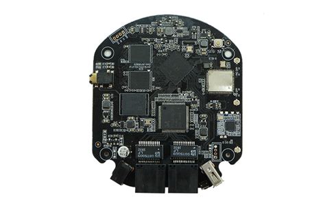
Advanced PCB Fabrication Equipment for Precision Manufacturing
Key Takeaways
When optimizing your PCB manufacturing operations, understanding core equipment capabilities directly impacts PCB manufacturing cost and production scalability. Modern laser-cut SMT stencils enable micron-level accuracy for solder paste application, reducing rework rates by up to 40% compared to traditional methods. For PCB manufacturing companies, integrating precision pick-and-place systems ensures component placement speeds exceeding 25,000 units per hour, critical for maintaining competitive lead times.
Industrial-grade reflow ovens with closed-loop thermal profiling minimize thermal stress, a common pain point in high-density designs. Below is a comparison of traditional vs. advanced fabrication approaches:
| Factor | Traditional Methods | Advanced Equipment |
|---|---|---|
| Setup Time | 4-6 hours | <1 hour |
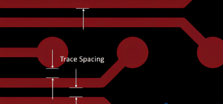
| Error Margin | ±0.2mm | ±0.05mm |
| Batch Flexibility | 50+ units | 1-50 units |
“Investing in multi-cavity tooling isn’t just about speed—it’s about creating redundancy for complex designs,” notes a leading industry analyst. This approach lets you parallelize prototyping phases, slashing PCB manufacturing business overhead by 30% for small-batch orders.
Laser cutting solutions further streamline workflows, achieving kerf widths under 20μm for RF and high-frequency boards. When paired with advanced milling systems, you gain the agility to pivot between prototypes and mid-volume runs without retooling delays—a strategic advantage in fast-paced markets. By prioritizing these innovations, you position your operation to tackle evolving PCB manufacturing cost challenges while scaling efficiently.
Laser-Cut SMT Stencil Technology
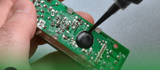
When optimizing PCB manufacturing workflows, laser-cut SMT stencils represent a critical advancement for achieving micron-level precision in solder paste deposition. Unlike traditional chemical etching methods, laser-cutting technology eliminates inconsistencies caused by undercutting, ensuring aperture walls remain smooth and vertical. This directly reduces defects like bridging or insufficient solder volume—common pain points for PCB manufacturing companies handling high-density designs.
Modern systems employ fiber lasers with ±10µm accuracy, allowing you to create stencils for components as small as 01005 packages or micro-BGA arrays. The process also supports rapid iterations, which is invaluable when balancing PCB manufacturing cost with prototyping speed. By integrating automated optical inspection (AOI) compatibility, these stencils ensure alignment perfection, even for double-sided or flexible PCB designs.
For PCB manufacturing businesses focused on small-batch production, the ability to swap stencils within minutes—coupled with reusable frames—translates to 25–40% faster setup times. This agility becomes a competitive edge when catering to industries like medical devices or IoT, where design changes occur frequently. When paired with advanced solder paste jetting systems, laser-cut stencils further minimize material waste, reinforcing their role in sustainable, high-yield manufacturing ecosystems.
Precision Pick-and-Place Automation
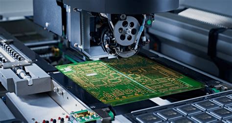
When optimizing PCB manufacturing workflows, precision pick-and-place systems redefine how components are positioned on boards with micron-level accuracy. Modern systems achieve placement speeds exceeding 25,000 components per hour while maintaining tolerances below ±25μm, ensuring consistent quality even for high-density designs. For PCB manufacturing companies, this automation reduces manual intervention, minimizing errors that escalate PCB manufacturing costs during rework phases.
Advanced machines integrate vision-guided alignment and real-time feedback loops to adapt to varying component sizes, from 0201 resistors to complex BGAs. By streamlining the assembly process, you gain flexibility to handle both prototyping runs and scaled production without recalibration delays—a critical advantage for PCB manufacturing businesses balancing speed and precision. Dual-lane conveyors and modular nozzle configurations further enhance throughput, allowing parallel processing of multiple board designs.
Transitioning to these systems also future-proofs operations, as software-driven platforms support AI-powered optimization for material utilization and cycle time reduction. Whether you’re assembling consumer electronics or industrial control systems, precision pick-and-place automation ensures your PCB manufacturing line remains competitive in markets demanding faster turnaround and tighter tolerances.
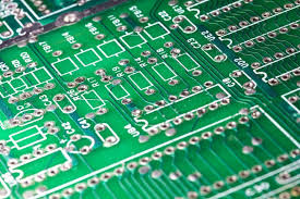
Industrial-Grade Reflow Oven Systems
When optimizing pcb manufacturing workflows, industrial-grade reflow ovens stand as critical assets for achieving repeatable solder joint quality in high-volume production. These systems employ precise thermal profiling, ensuring even heat distribution across pcb manufacturing business assemblies—whether you’re working with lead-free solders or complex multi-layer boards. Advanced models integrate nitrogen-rich environments to minimize oxidation, a feature particularly valuable for pcb manufacturing companies handling fine-pitch components or sensitive IoT devices.
Modern reflow ovens automate temperature ramps and cooling cycles, slashing pcb manufacturing cost by reducing manual adjustments and minimizing defects like tombstoning or cold joints. Their modular designs allow scalability, supporting everything from rapid prototyping to full-scale production lines. For businesses balancing quality and throughput, dual-zone configurations enable simultaneous processing of different board types without cross-contamination. By pairing these systems with precision pick-and-place automation, you create a closed-loop process where component placement accuracy aligns perfectly with thermal requirements—a synergy that elevates both yield rates and end-product reliability.
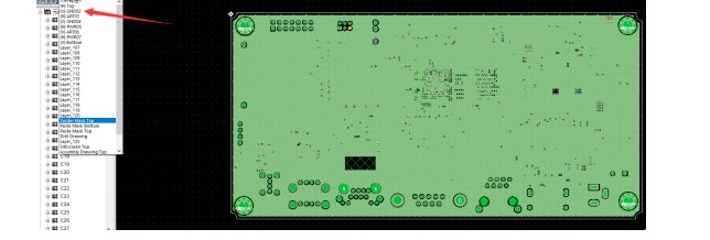
Advanced Milling for PCB Prototyping
When optimizing PCB manufacturing workflows, advanced milling systems play a pivotal role in accelerating prototyping cycles. Modern CNC milling equipment enables PCB manufacturing companies to achieve tolerances as tight as ±0.001”, ensuring precise trace routing and via formation without the delays of traditional etching. These systems integrate adaptive depth control, automatically adjusting spindle speed to handle diverse substrates—from standard FR-4 to high-frequency Rogers materials.
For startups or businesses managing PCB manufacturing cost, desktop milling machines offer a cost-effective entry point. Unlike outsourced production, in-house milling eliminates tooling fees and reduces lead times for design iterations. However, balancing speed and precision remains critical: higher spindle speeds (up to 100,000 RPM) minimize burring, while vacuum workholding stabilizes thin laminates during micro-machining.
Advanced systems also support multi-layer alignment through optical fiducial recognition, a feature increasingly vital for complex HDI designs. By integrating milling into your PCB manufacturing business, you bypass photolithography steps, reducing chemical waste and material scrap rates by up to 30%. This approach not only streamlines prototyping but also scales efficiently for low-volume batches, bridging the gap between R&D and full-scale production.
Laser Cutting Solutions for PCBs
When optimizing PCB manufacturing workflows, laser cutting systems have become indispensable for achieving micron-level accuracy in circuit board production. Unlike mechanical drilling or traditional etching methods, fiber lasers and UV lasers deliver clean, burr-free cuts on substrates ranging from FR-4 to flexible polyimide, ensuring minimal thermal stress on sensitive components. For PCB manufacturing companies, this translates to faster turnaround times for high-density interconnect (HDI) designs and rigid-flex boards, directly addressing challenges in PCB manufacturing cost control.
Modern systems integrate vision-guided alignment to handle panels with ±5μm precision, enabling seamless processing of complex geometries like castellated holes or fine-pitch traces. This capability is particularly valuable for prototyping, where iterative design changes demand rapid adjustments without retooling expenses. By reducing material waste and eliminating secondary finishing steps, laser technology strengthens the competitiveness of your PCB manufacturing business in markets requiring quick adaptation to IoT or 5G hardware demands.
For mixed-material boards, hybrid laser systems combine CO2 and UV wavelengths to process copper, solder mask, and dielectric layers in a single pass—a critical advantage when balancing speed with precision. As layer counts increase in advanced electronics, these solutions ensure consistent quality while scaling from small batches to mid-volume production runs.
Multi-Cavity Tooling Efficiency
When optimizing PCB manufacturing workflows, multi-cavity tooling stands out as a game-changer for balancing speed and precision. By employing molds that produce multiple identical boards in a single cycle, cycle times drop significantly while throughput scales proportionally. For PCB manufacturing companies handling complex designs or high-volume orders, this method reduces PCB manufacturing cost by minimizing material waste and labor hours—critical factors in maintaining competitive pricing.
Advanced multi-cavity systems integrate with automated workflows, ensuring consistent alignment across cavities even for designs requiring tight tolerances. This efficiency is particularly valuable in the PCB manufacturing business, where rapid turnaround for prototypes and small batches can make or break client relationships. While initial tooling investments may appear steep, the long-term savings from reduced per-unit costs and faster production cycles justify the upfront expenditure.
Transitioning to multi-cavity solutions also future-proofs operations, allowing seamless scaling as demand grows. Whether you’re producing intricate aerospace boards or consumer electronics, leveraging this technology ensures your processes stay agile in fast-paced markets—a strategic advantage when every second counts.
Streamlined Small-Batch Production
When optimizing for PCB manufacturing of limited quantities, efficiency hinges on balancing precision with flexibility. Modern pcb manufacturing companies leverage modular equipment configurations that eliminate the need for costly retooling, enabling rapid transitions between designs. By integrating adaptive laser cutting systems and multi-cavity tooling, you reduce pcb manufacturing cost while maintaining tight tolerances—even for complex, high-density layouts.
Advanced software platforms now automate material utilization calculations, minimizing waste during prototyping. This approach not only accelerates turnaround times but also allows you to test multiple iterations without inflating expenses. For pcb manufacturing business models prioritizing agility, industrial-grade milling machines with real-time calibration ensure consistent quality across batches as small as 10 units.
The latest pick-and-place systems further streamline workflows by supporting mixed-component placement in a single run, bypassing traditional setup delays. Pairing these with cloud-connected reflow ovens creates a closed-loop process where thermal profiles adjust dynamically to board specifications. Such innovations let you scale production seamlessly, whether fulfilling niche orders or refining designs before mass production. By prioritizing adaptable technologies, small-batch workflows become a strategic asset rather than a cost burden.
PCB Fabrication Equipment Innovations
Modern advancements in PCB manufacturing equipment are reshaping how PCB manufacturing companies approach production challenges. Innovations like adaptive laser systems now enable micron-level accuracy for intricate circuit patterns, while AI-driven inspection tools reduce defects by analyzing real-time imaging data. These technologies directly address PCB manufacturing cost concerns by minimizing material waste and rework cycles. For businesses managing PCB manufacturing business operations, modular equipment designs offer scalability, allowing seamless transitions between prototyping and mid-volume runs without major capital investments.
A key breakthrough lies in hybrid additive-subtractive platforms, which combine 3D printing of conductive traces with precision milling to create multilayer boards in a single setup. This integration slashes turnaround times by up to 40% compared to traditional workflows. Additionally, closed-loop thermal management in modern reflow systems ensures consistent solder joint quality across batches—a critical factor for aerospace and medical-grade applications. By adopting these innovations, manufacturers achieve tighter process controls, transforming PCB manufacturing cost structures while meeting evolving industry standards for miniaturization and signal integrity.
Conclusion
When optimizing your PCB manufacturing operations, the strategic selection of pcb fabrication equipment directly impacts both quality and scalability. By integrating technologies like laser-cut stencils and automated pick-and-place systems, pcb manufacturing companies can reduce pcb manufacturing cost while maintaining precision—especially critical for prototyping and small-batch production. Industrial-grade reflow ovens and multi-cavity tooling further enhance throughput, enabling your pcb manufacturing business to meet diverse client demands without compromising turnaround times.
Advanced milling and laser-cutting solutions not only streamline workflows but also minimize material waste, aligning with cost-efficiency goals. As competition intensifies, investing in modern equipment becomes a differentiator, allowing you to balance high-volume capabilities with the flexibility required for niche projects. Ultimately, the right tools empower your facility to adapt to evolving industry standards while maintaining margins in a price-sensitive market.
Frequently Asked Questions
What factors influence pcb manufacturing cost for small-batch production?
Material selection, layer count, and surface finishes significantly impact pcb manufacturing cost. Advanced equipment like laser-cut SMT stencils and multi-cavity tooling reduces waste, optimizing expenses for prototypes or limited runs.
How do pcb manufacturing companies ensure precision in complex designs?
Leading firms integrate precision pick-and-place systems and industrial-grade reflow ovens to maintain micron-level accuracy. Automated optical inspection (AOI) systems further validate quality, critical for high-density interconnects.
Can modern pcb fabrication equipment improve turnaround times?
Yes. Laser cutting solutions and advanced milling machines accelerate prototyping, while modular tooling supports rapid design iterations. This efficiency is vital for pcb manufacturing business models prioritizing speed-to-market.
What equipment upgrades reduce long-term costs in pcb manufacturing?
Investing in multi-cavity tooling and automated depaneling systems minimizes manual labor. Additionally, energy-efficient reflow ovens lower operational expenses, enhancing ROI for high-mix production.
Why partner with specialized pcb manufacturing companies for prototyping?
Expert providers combine cutting-edge machinery with engineering support, ensuring design-for-manufacturability (DFM) compliance. This collaboration reduces errors and streamlines transitions to volume production.
Ready to Optimize Your PCB Production?
For tailored solutions that balance pcb manufacturing cost with precision, please click here to explore industrial-grade equipment and technical support for your pcb manufacturing business.