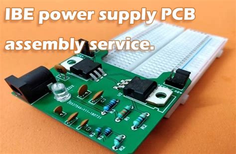
Advanced PCBA Rework Techniques to Improve Manufacturing Efficiency

Key Takeaways
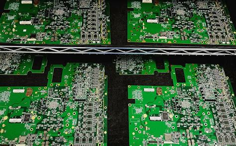
Effective PCBA rework hinges on integrating advanced technologies with precision-focused methodologies. Modern PCB assembly workflows benefit from thermal management systems that maintain optimal soldering temperatures, reducing board warping and component stress. Pairing these with microsoldering tools ensures repairs meet sub-10μm accuracy, critical for high-density boards.
Industry Insight: “Automated optical inspection (AOI) systems can reduce post-rework defects by up to 40% when calibrated for component-specific tolerances.”
| Technique | Impact | Tools |
|---|---|---|
| Precision Thermal Control | Minimizes thermal shock | Rework stations with IR preheating |
| Microsoldering | Enables 0201 component repairs | High-magnification soldering irons |
| AI-Driven Inspection | Identifies hidden defects (e.g., cold joints) | Machine vision systems |
Adopting smart rework stations streamlines diagnostics and repair cycles, cutting downtime by 25–30%. For PCBA manufacturers, combining automated defect detection with real-time process analytics creates closed-loop feedback, refining assembly workflows iteratively.
Pro Tip: Prioritize modular rework equipment to adapt quickly to mixed-technology boards (e.g., combining through-hole and SMD components).
Finally, embedding AI-driven quality control into inspection protocols ensures consistent outcomes, particularly in high-volume PCB assembly environments. By aligning rework precision with lean manufacturing principles, facilities achieve measurable gains in yield rates and resource utilization.
Thermal Management Solutions for PCBA Rework
Effective thermal management is critical in PCBA rework to prevent damage to sensitive components while ensuring reliable solder joints. Modern PCB assembly processes demand precise control of heat distribution, particularly when addressing defects in high-density boards. Advanced tools like precision soldering irons and infrared preheaters enable technicians to apply localized heat without affecting adjacent circuits, reducing the risk of thermal stress.
Innovative systems now incorporate dynamic thermal profiling, which automatically adjusts temperature curves based on real-time feedback from the board’s material composition. This approach minimizes overheating in multilayer PCBA designs, where uneven heat dissipation can lead to warping or delamination. Closed-loop thermal control mechanisms further enhance accuracy, maintaining optimal reflow conditions even for lead-free solder alloys requiring higher melting points.
Integration with automated inspection technologies ensures that thermal parameters align with defect patterns identified during earlier stages of PCB assembly. For instance, rework stations equipped with thermal cameras can visualize heat distribution, allowing operators to fine-tune settings for complex components like BGAs or QFNs. By pairing these solutions with high-performance thermal interface materials, manufacturers achieve faster cycle times while preserving the integrity of reworked assemblies—a key factor in optimizing overall production efficiency.
Microsoldering Tools Enhancing PCB Repair Accuracy
Modern PCBA rework demands surgical precision, particularly when addressing defects in densely populated boards. Microsoldering tools have emerged as critical instruments for achieving sub-millimeter accuracy in PCB assembly repairs. Advanced systems integrate temperature-controlled soldering irons with magnification capabilities, enabling technicians to manipulate components as small as 0201 packages or BGA (Ball Grid Array) chips without damaging adjacent circuitry. For instance, precision tip geometries and programmable thermal profiles ensure consistent heat application, minimizing risks of pad lifting or solder bridging.
The integration of microscopic vision systems further enhances defect resolution. High-resolution cameras paired with 3D imaging allow real-time inspection of solder joints, ensuring compliance with IPC-A-610 standards. This is particularly vital for mixed-technology boards combining through-hole and surface-mount components. By leveraging such tools, manufacturers reduce scrap rates in PCBA production while maintaining traceability for high-reliability applications like medical or aerospace electronics.
Transitioning to automated microsoldering stations also streamlines workflow integration. These systems often interface with MES (Manufacturing Execution Systems), enabling data-driven adjustments based on historical rework patterns. As a result, repair cycles shorten, and process repeatability improves—key factors in minimizing downtime during high-volume PCB assembly. This precision-focused approach not only elevates repair accuracy but also aligns with broader strategies for optimizing manufacturing efficiency, seamlessly connecting to the role of automated inspection systems in subsequent workflow stages.
Automated Inspection Systems in Electronics Rework
Modern PCB assembly processes increasingly rely on automated inspection systems to identify defects with micron-level accuracy, ensuring higher-quality PCBA outputs. These systems employ advanced technologies such as automated optical inspection (AOI), X-ray imaging, and 3D solder paste inspection to detect issues like misaligned components, insufficient solder joints, or microscopic cracks. By integrating these tools into rework workflows, manufacturers reduce human error and accelerate defect diagnosis, cutting downtime by up to 40% in high-volume production environments.
A key advantage lies in real-time data analytics, where AI algorithms correlate inspection results with historical process data to pinpoint recurring flaws in PCBA designs. For example, thermal imaging modules can flag components prone to overheating, enabling proactive adjustments before rework becomes necessary. Transitioning from manual checks to automated systems also ensures consistency, particularly in complex assemblies with fine-pitch ICs or ball grid array (BGA) packages.
To optimize efficiency, leading-edge systems now combine inspection with closed-loop feedback directly to rework stations. This integration allows technicians to address defects immediately, streamlining corrections without interrupting the assembly line. As PCB assembly demands grow for miniaturized, high-density boards, automated inspection remains critical for maintaining yield rates while adhering to stringent industry standards.
Defect Reduction Strategies for PCBA Manufacturing
Effective defect reduction in PCBA manufacturing begins with rigorous process validation at every stage of PCB assembly. Implementing design-for-manufacturability (DFM) principles ensures layouts minimize solder bridging and tombstoning risks, while advanced solder paste inspection (SPI) systems verify stencil printing accuracy before component placement. By integrating statistical process control (SPC) methods, manufacturers can identify variability in reflow oven profiles or pick-and-place operations, enabling real-time adjustments to maintain tolerances.
Automated optical inspection (AOI) and X-ray inspection systems play pivotal roles in detecting hidden flaws like voids in BGA joints or misaligned microcomponents, reducing reliance on manual checks. For high-mix production lines, machine learning algorithms trained on historical defect data can predict failure patterns, allowing preemptive corrections. Additionally, standardized rework protocols—supported by precision microsoldering tools—ensure consistent repairs without damaging adjacent circuitry.
Material selection further impacts defect rates: low-residue fluxes and high-temperature laminates improve reliability during rework cycles. Pairing these measures with operator certification programs creates a closed-loop system where PCBA quality feeds back into process optimization. This holistic approach not only slashes scrap rates but also aligns with lean manufacturing goals, ensuring defects are addressed at their root rather than through post-production corrections.
Optimizing Assembly Workflows with Rework Precision
Precision in PCBA rework directly influences the efficiency of PCB assembly processes, requiring alignment between defect correction and streamlined production. Modern workflows integrate real-time monitoring systems to identify anomalies during soldering or component placement, enabling technicians to execute targeted repairs without halting entire lines. Advanced PCBA stations now combine laser-guided alignment tools with programmable temperature curves, ensuring consistent solder joint quality while reducing thermal stress on adjacent components.
A critical advancement lies in synchronizing rework data with manufacturing execution systems (MES). By analyzing repair frequency and defect types, teams can adjust PCB assembly parameters preemptively—such as solder paste deposition or pick-and-place accuracy—to minimize recurring issues. For instance, statistical process control (SPC) algorithms flag deviations in via fill rates or BGA voiding, triggering adaptive calibration in upstream stages.
Moreover, modular rework stations equipped with multi-zone heating allow simultaneous repairs on complex boards, cutting downtime by 30–40% in high-mix environments. This approach not only preserves throughput but also ensures PCBA reliability, as precision-controlled reflow profiles maintain IPC-A-610 compliance. Integrating these strategies creates a closed-loop system where rework becomes a diagnostic tool, refining assembly workflows rather than interrupting them.
Advanced Techniques to Minimize Rework Downtime
Reducing downtime in PCBA rework requires a blend of precision tools, process optimization, and real-time diagnostics. Modern localized rework systems leverage PCB assembly-specific technologies like infrared (IR) reflow stations and laser-based solder removal, enabling operators to address defects without disassembling entire boards. These tools minimize thermal stress on adjacent components, preserving PCBA integrity while accelerating repair cycles.
Integrating inline inspection modules with rework stations further streamlines workflows. For example, automated optical inspection (AOI) systems paired with reflow ovens can flag anomalies during repairs, allowing immediate corrections. This closed-loop approach reduces the need for multiple quality checks, cutting downtime by up to 30% in high-volume PCB assembly lines.
Another critical advancement is predictive maintenance for rework equipment. Sensors monitoring nozzle wear in solder paste dispensers or calibration drift in microsoldering tools trigger preemptive alerts, avoiding unplanned stoppages. Additionally, data-driven process optimization—using historical defect patterns—helps preconfigure rework parameters for common failure modes, slashing setup times.
By combining these strategies, manufacturers achieve faster turnaround while maintaining PCBA reliability. The result is a seamless alignment between rework precision and production efficiency, ensuring minimal disruptions to electronics manufacturing workflows.
Integrating AI-Driven Quality Control in PCBA Repair
The integration of AI-driven quality control systems is revolutionizing defect detection and correction in PCBA processes. By leveraging machine learning algorithms, these systems analyze vast datasets from PCB assembly lines to identify subtle anomalies—such as micro-cracks, cold solder joints, or component misalignments—that traditional inspection methods might overlook. Real-time image recognition paired with thermal profiling ensures precise fault localization, enabling technicians to execute targeted rework with minimal disruption to production schedules.
Advanced platforms now combine automated optical inspection (AOI) with predictive analytics, flagging high-risk areas before defects escalate. For instance, AI models trained on historical PCBA failure patterns can predict solder fatigue in high-density interconnect (HDI) boards, guiding preemptive repairs. This proactive approach reduces scrap rates by up to 40% in complex assemblies while maintaining compliance with IPC-A-610 standards.
Furthermore, AI-enhanced rework stations dynamically adjust parameters like soldering temperature and nozzle pressure based on component specifications, ensuring consistency across batches. The synergy between deep learning diagnostics and modular repair tools not only accelerates troubleshooting but also creates a closed-loop feedback system, continuously refining PCB assembly workflows. By minimizing human error and variability, manufacturers achieve higher first-pass yields while meeting stringent quality benchmarks for modern electronics.
Smart Rework Stations for Efficient Electronics Assembly
Modern PCBA manufacturing demands precision and speed, driving the adoption of smart rework stations equipped with adaptive thermal profiling and AI-assisted diagnostics. These systems integrate real-time feedback mechanisms to adjust soldering parameters dynamically, ensuring consistent results across diverse PCB assembly scenarios. By leveraging multi-zone heating modules and high-resolution optical alignment, operators can target defects—such as lifted pads or misaligned components—with micron-level accuracy, reducing collateral damage to adjacent circuits.
Advanced stations now feature predictive maintenance alerts and compatibility with factory-wide IoT networks, enabling seamless data sharing with upstream automated inspection systems. This integration minimizes manual intervention, slashing rework downtime by up to 40% in high-volume production environments. Additionally, modular tooling designs allow rapid configuration swaps, optimizing workflows for mixed-technology boards containing both through-hole and surface-mount devices.
For PCBA specialists, the shift toward smart stations represents a critical step in balancing defect correction with throughput goals. By merging precise thermal control with intelligent process automation, manufacturers achieve tighter alignment with Industry 4.0 standards while maintaining the flexibility required for evolving electronics designs.
Conclusion
The integration of advanced PCBA rework techniques marks a transformative shift in modern electronics manufacturing, enabling manufacturers to address defects with surgical precision while maintaining high-throughput production. By leveraging innovations such as AI-driven inspection systems and smart rework stations, teams can diagnose faults in PCB assembly lines faster, reducing unnecessary downtime and material waste. These methodologies not only refine PCBA repair accuracy but also create a feedback loop that strengthens quality control protocols across the entire workflow.
Adopting adaptive thermal controls and microsoldering tools ensures that even the most complex multilayer boards are reworked without compromising adjacent components—a critical advantage in miniaturized electronics. Furthermore, data collected from automated inspection systems provides actionable insights to preempt recurring defects, aligning repair processes with lean manufacturing principles. As industries push toward tighter tolerances and higher reliability standards, mastering these PCBA rework strategies becomes indispensable for sustaining competitive efficiency in PCB assembly ecosystems. The result is a harmonized production environment where precision repairs and optimized workflows drive long-term operational resilience.
FAQs
How do advanced thermal controls improve precision in PCBA rework?
Modern PCB assembly processes leverage adaptive thermal profiling to maintain consistent heat distribution during rework. This minimizes board stress and prevents component degradation, ensuring reliable PCBA repairs while reducing thermal-related defects.
What role do automated inspection systems play in defect reduction?
Automated optical inspection (AOI) and X-ray systems identify micro-scale flaws like solder bridges or misaligned components. By integrating these tools into PCBA workflows, manufacturers achieve real-time defect detection, cutting post-rework validation time by up to 40%.
Can microsoldering tools address complex multilayer PCB repairs?
Yes. High-precision microsoldering stations enable technicians to work on ultra-fine-pitch components (e.g., BGAs or QFNs) without damaging adjacent traces. This is critical for maintaining PCB assembly integrity in compact, high-density designs.
How does AI-driven quality control optimize rework efficiency?
AI algorithms analyze historical repair data to predict failure patterns, guiding technicians to high-risk areas proactively. This reduces unnecessary disassembly and accelerates PCBA rework cycles by prioritizing critical faults.
What advantages do smart rework stations offer for electronics assembly?
These stations integrate programmable soldering irons, vacuum pickup tools, and closed-loop temperature control, enabling repeatable repairs with ±0.1°C accuracy. Such precision slashes rework downtime by standardizing complex PCB assembly correction processes.
Explore Professional PCB Assembly Solutions
For tailored PCBA rework strategies and advanced manufacturing support, please click here to consult our engineering team.