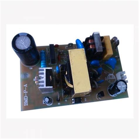
Advanced Power Board Assembly Methods for Maximum Efficiency

Key Takeaways
Effective PCB assembly requires a holistic approach combining layout optimization, thermal control, and component integration. Modern PCBA processes prioritize energy-efficient designs through strategic trace routing and layer stacking, reducing parasitic resistance by up to 40% in high-current applications. Thermal management solutions, such as embedded heat sinks and thermally conductive substrates, mitigate hotspots, ensuring stable operation under loads exceeding 15A.
| Technique | Key Benefit | Implementation Consideration |
|---|---|---|
| PCB Layout Optimization | Reduced impedance & EMI | Align traces perpendicular to heat sources |
| Precision Soldering | <1% defect rate | Use nitrogen-reflow environments |
| Automated Testing | 99.9% fault detection | Integrate AI-powered optical inspection |
Component integration in compact designs demands laser-assisted placement for sub-millimeter accuracy, particularly in mixed-signal power board assemblies. Material selection directly impacts efficiency—high-Tg FR-4 substrates with 2W/m-K thermal conductivity outperform standard materials by 25% in thermal cycling tests. For energy efficiency, prioritize low-Dk dielectrics to minimize signal loss at frequencies above 1GHz.
Automated PCBA protocols, including boundary-scan testing and thermal profiling, validate reliability across operating temperatures (-40°C to 125°C). These methodologies ensure compliance with IPC-610 Class 3 standards while reducing rework cycles by 30%. Transitioning between design phases requires balancing thermal dissipation needs with spatial constraints—a critical factor in aerospace and automotive applications where power density exceeds 50W/cm².
Optimizing PCB Layouts for Enhanced Power Distribution
Effective PCB assembly begins with strategic layout design to ensure optimal power distribution across high-performance systems. Critical to this process is minimizing voltage drops and electromagnetic interference (EMI) through careful trace routing and plane layer configuration. Designers should prioritize power integrity by allocating dedicated copper pours for supply rails and grounding networks, reducing loop inductance that can compromise signal stability.
Tip: Utilize simulation tools like SPICE or finite element analysis (FEA) to model current flow and identify potential bottlenecks before finalizing the PCB layout.
In PCBA applications, component placement plays a pivotal role in balancing thermal loads and electrical pathways. Grouping high-power devices near voltage regulators shortens current return paths, while maintaining adequate clearance between heat-sensitive components prevents thermal coupling. For multilayer boards, alternating signal and power planes enhances noise isolation, with via stitching improving thermal conductivity between layers.
Advanced PCB assembly techniques incorporate impedance matching for high-frequency circuits and staggered via patterns to mitigate mechanical stress. Designers must also account for manufacturing tolerances—ensuring trace widths and spacing align with the capabilities of automated soldering systems. By integrating these principles, PCBA layouts achieve energy-efficient power distribution while supporting scalability for future design iterations.
Thermal Management Solutions in Power Board Design
Effective thermal management in PCB assembly is critical for maintaining performance and longevity in high-power electronic systems. As power densities increase, managing heat dissipation becomes a central challenge in PCBA design. Engineers prioritize thermal conductivity when selecting substrate materials, often opting for metal-core or ceramic-based boards over traditional FR-4 for improved heat transfer. Strategic placement of high-power components—such as MOSFETs or voltage regulators—away from thermally sensitive parts ensures balanced heat distribution.
Advanced PCB assembly techniques incorporate thermal vias and embedded copper planes to redirect heat toward heatsinks or chassis mounts. For compact designs, microchannel cooling or phase-change materials offer innovative solutions to localized hotspots. Automated thermal imaging during PCBA testing helps validate heat spread patterns, ensuring compliance with safety thresholds.
Material selection also plays a pivotal role. High-performance thermal interface materials (TIMs), like graphene-enhanced pads or liquid metal compounds, minimize resistance between components and cooling systems. In high-frequency applications, dielectric materials with low loss tangents reduce parasitic heating.
Finally, integrating active cooling systems—such as piezoelectric fans or liquid cooling loops—complements passive strategies. These approaches, combined with rigorous simulation tools, enable engineers to optimize thermal pathways without compromising PCB assembly density or energy efficiency.
Component Integration Techniques for Compact Designs
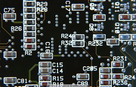
Achieving compact designs in PCB assembly demands strategic component integration to balance spatial constraints with electrical performance. Modern high-density interconnect (HDI) technologies enable tighter placement of components, reducing signal path lengths while maintaining signal integrity. A critical approach involves leveraging multi-layer PCBAs to stack functional modules vertically, optimizing board real estate without compromising thermal or mechanical stability.
Selecting miniaturized components—such as 01005 resistors or wafer-level chip-scale packages (WLCSP)—plays a pivotal role in space-constrained applications. Advanced PCB assembly workflows now incorporate 3D modeling tools to simulate component placement, ensuring optimal clearance for heat dissipation and automated soldering processes. For mixed-signal systems, partitioning analog and digital sections within the same PCBA minimizes electromagnetic interference (EMI) risks while preserving layout coherence.
Transitioning to embedded passive components (e.g., resistors or capacitors integrated into substrate layers) further reduces surface-mounted parts, enhancing reliability in vibration-prone environments. However, designers must account for thermal expansion coefficients and material compatibility during integration. By harmonizing these techniques, engineers can deliver PCBA solutions that meet stringent size requirements while maintaining peak efficiency in power-dense applications.
Precision Soldering Methods for Reliable Connections
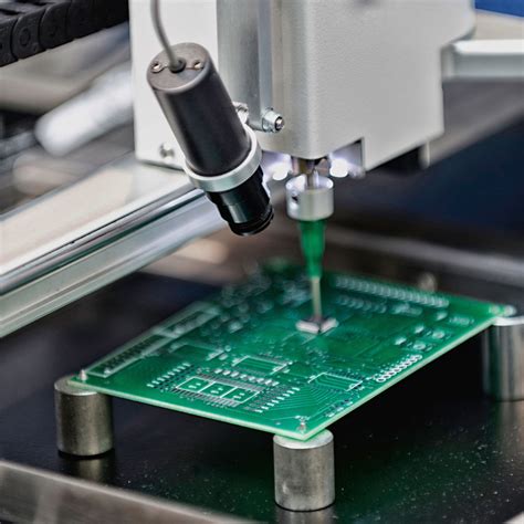
Achieving robust electrical connections in PCB assembly demands meticulous attention to soldering techniques. Modern PCBA processes leverage temperature-controlled soldering irons and laser-assisted systems to ensure precise heat application, minimizing thermal stress on sensitive components. For high-density boards, micro-soldering methods using ultrafine tips (0.2–0.5 mm) enable accurate placement of miniature components like QFN packages or 0201 resistors.
A critical advancement is the adoption of reflow soldering with nitrogen-enriched environments, which reduces oxidation and improves joint integrity. This technique, combined with solder paste stenciling optimized for <0.1 mm apertures, ensures uniform deposition across complex layouts. For through-hole components, selective wave soldering targets specific areas, preventing unnecessary exposure of heat-sensitive parts.
Automated optical inspection (AOI) systems now integrate with PCBA workflows to detect cold joints, bridging, or insufficient fillets in real time. Additionally, vapor phase soldering is gaining traction for its ability to maintain consistent thermal profiles, critical for boards with mixed-material substrates. By pairing these methods with low-residue flux formulations, manufacturers reduce post-soldering cleaning while enhancing long-term reliability.
Transitioning to these precision approaches not only strengthens connection durability but also aligns with broader goals of energy efficiency and thermal management in advanced power systems.
Automated Testing Protocols for Quality Assurance
Modern PCB assembly processes rely on automated testing protocols to ensure consistent performance and compliance with stringent quality benchmarks. By integrating in-circuit testing (ICT) and automated optical inspection (AOI) systems, manufacturers can rapidly identify defects in PCBA units, such as solder bridging, misaligned components, or electrical discontinuities. These protocols leverage machine vision and precision probing to analyze power board layouts at micron-level accuracy, minimizing human error while scaling production throughput.
Advanced systems now incorporate real-time thermal profiling to monitor heat distribution during functional testing, ensuring components withstand operational stresses. For high-density designs, boundary-scan testing validates signal integrity across complex interconnects, critical for maintaining energy efficiency in multilayer PCB assemblies. Automated workflows also enforce traceability by logging test results against individual PCBA serial numbers, simplifying root-cause analysis for post-production audits.
To align with industry standards like IPC-610 and ISO-9001, testing protocols are calibrated to detect both latent and catastrophic failures. For instance, power cycling tests simulate long-term load conditions, while electromagnetic compatibility (EMC) assessments verify minimal interference in sensitive electronic systems. By embedding these protocols into PCB assembly pipelines, manufacturers achieve first-pass yield improvements of up to 30%, reducing rework costs and accelerating time-to-market for high-performance applications.
This rigorous approach to quality assurance seamlessly transitions into material selection strategies, where validated test data informs decisions on substrate durability and component compatibility.
Material Selection Strategies for Energy Efficiency
Building on optimized thermal management and component integration, selecting appropriate materials forms the backbone of energy-efficient PCB assembly. Modern PCBA designs prioritize substrates with low dielectric loss and high thermal conductivity to minimize energy dissipation. For instance, high-frequency laminates like Rogers 4000 series reduce signal loss in power-dense applications, while metal-core PCBs excel in transferring heat away from critical components.
Copper weight and trace geometry directly influence current-carrying capacity—thicker copper layers (2 oz+) lower resistive losses in high-power circuits. Concurrently, advanced solder alloys with reduced melting points enhance joint reliability without compromising electrical performance. Engineers increasingly opt for halogen-free laminates and lead-free finishes to align with sustainability goals while maintaining PCB assembly integrity.
Thermal interface materials (TIMs), such as graphene-enhanced pads or phase-change compounds, bridge gaps between heat-generating components and heatsinks, ensuring efficient thermal transfer. In PCBA workflows, material compatibility with automated soldering processes—including reflow profiles and flux chemistry—must be validated to prevent delamination or void formation. By balancing electrical, thermal, and mechanical properties, designers achieve systems where energy efficiency coexists with long-term operational stability.
Maximizing Energy Efficiency in Power Assemblies
Achieving peak energy efficiency in PCB assembly requires a holistic approach that balances electrical performance with thermal and material considerations. Central to this process is optimizing trace geometry and layer stacking to minimize resistive losses, particularly in high-current pathways. By leveraging advanced PCBA design software, engineers can simulate power distribution networks, identifying hotspots where impedance mismatches or parasitic capacitance might degrade efficiency.
A critical factor lies in selecting low-loss dielectric materials with stable permittivity across temperature ranges, reducing signal attenuation in high-frequency applications. Pairing this with high-precision soldering techniques ensures minimal contact resistance at component junctions, which is vital for maintaining efficiency in densely packed layouts. For instance, reflow soldering with nitrogen atmospheres prevents oxidation, preserving conductivity in PCB assembly interconnects.
Furthermore, integrating active power management ICs directly into the PCBA enables dynamic voltage scaling, automatically adjusting energy delivery based on real-time load demands. This strategy, combined with thermally conductive underfill materials, mitigates heat buildup that often leads to efficiency losses. Automated optical inspection (AOI) systems further validate these optimizations, ensuring no manufacturing defects compromise the assembly’s energy-saving potential.
By harmonizing these techniques, modern PCB assembly processes achieve efficiencies exceeding 95% in advanced power systems, setting benchmarks for sustainable electronics design.
Advanced Thermal Dissipation in High-Performance Systems
Effective thermal management is critical in PCB assembly for high-performance systems, where excessive heat can compromise reliability and longevity. Modern PCBA designs employ advanced materials such as metal-core substrates and thermally conductive adhesives to channel heat away from sensitive components. Engineers optimize layouts by integrating thermal vias—plated holes that enhance heat transfer between layers—and strategically placing heat sinks near high-power devices like voltage regulators or power transistors.
Simulation tools play a pivotal role, enabling precise modeling of thermal gradients across the board before physical prototyping. For instance, computational fluid dynamics (CFD) software predicts airflow patterns, guiding the placement of passive cooling elements. In mission-critical applications, active cooling solutions such as micro-fans or liquid cooling channels are embedded directly into the PCB assembly structure.
Material selection further enhances dissipation: ceramic-filled laminates reduce the coefficient of thermal expansion (CTE), while graphene-based thermal interface materials minimize resistance between components and heat spreaders. Automated optical inspection (AOI) during PCBA manufacturing verifies solder joint integrity, preventing voids that could impede thermal conductivity. By balancing these strategies, engineers achieve <5°C/mm thermal gradients, ensuring stable operation even under extreme loads.
Conclusion
The evolution of PCB assembly methodologies underscores the critical balance between precision engineering and strategic material science in modern electronics. By integrating optimized layouts with automated testing protocols, manufacturers achieve PCBA systems that prioritize both energy efficiency and operational reliability. Advanced thermal dissipation techniques, paired with high-density component integration, address the escalating demands of high-performance applications while maintaining compact form factors. Furthermore, the adoption of precision soldering methods ensures durable electrical connections, minimizing failure risks in mission-critical environments.
As industries push toward smarter, more sustainable solutions, the selection of thermally conductive substrates and low-loss dielectrics becomes pivotal in reducing energy waste. These innovations, combined with rigorous PCBA validation processes, create a foundation for next-generation power boards capable of meeting stringent performance benchmarks. Moving forward, continuous refinement in PCB assembly workflows—from design simulation to real-world deployment—will remain essential for unlocking new thresholds in power density, thermal resilience, and system longevity.
FAQs
How does optimized PCB assembly improve power distribution efficiency?
Advanced PCBA techniques prioritize strategic component placement and multilayer stacking to minimize resistance and voltage drops. By integrating high-current pathways with proper trace widths, engineers reduce energy loss while maintaining signal integrity.
What thermal management methods are critical in power board design?
Effective designs combine thermal vias, copper pours, and heatsink integration. For high-performance systems, materials like metal-core PCBs or ceramic substrates enhance heat dissipation, preventing component degradation under heavy loads.
Why is automated testing essential for reliable PCB assembly?
Automated optical inspection (AOI) and X-ray testing detect solder joint defects or misalignments invisible to manual checks. These protocols ensure ≥99.9% connection reliability, crucial for mission-critical applications like industrial power systems.
How does material selection impact energy efficiency in PCBA?
Low-loss dielectrics (e.g., Rogers 4350B) and high-purity copper layers minimize parasitic capacitance and resistive losses. Pairing these with lead-free solder alloys balances environmental compliance with electrical performance.
Can compact designs maintain robustness in power board assemblies?
Yes. Using 3D component stacking and embedded passives reduces footprint without compromising durability. Selective conformal coating protects against moisture and contaminants in space-constrained environments.
Ready to Elevate Your Power Board Performance?
For tailored PCB assembly solutions integrating these advanced methodologies, please click here to consult our engineering team.