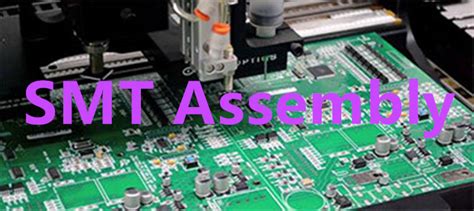
Advanced SMT Assembly Solutions for Modern PCB Manufacturing
Key Takeaways
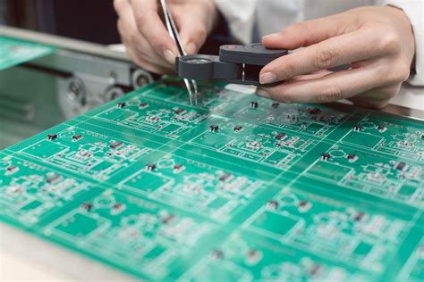
Modern PCB assembly processes leverage precision automation to achieve micron-level accuracy in component placement, particularly critical for miniaturized components in IoT devices and wearables. Advanced PCBA solutions now integrate AI-driven quality control systems that perform real-time defect detection, reducing error rates by up to 65% compared to manual inspections. These innovations are reshaping industries, from automotive-grade assemblies requiring -40°C to 150°C operational stability to industrial electronics demanding zero-defect production for mission-critical systems.
The shift toward high-density interconnect (HDI) designs in PCB assembly underscores the importance of solder paste inspection (SPI) and automated optical inspection (AOI) in PCBA workflows. For automotive applications, traceability protocols ensure compliance with IATF 16949 standards, while industrial IoT deployments benefit from edge-computing-ready SMT modules. As manufacturers adopt Industry 4.0 practices, predictive maintenance algorithms are optimizing pick-and-place machinery uptime, directly enhancing throughput in high-mix production environments. These advancements position SMT assembly services as the backbone of next-generation electronics manufacturing.
Precision Automation in SMT Assembly
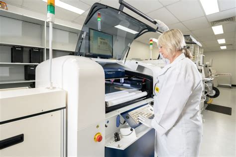
Modern PCB assembly processes rely heavily on precision automation to meet the escalating demands for speed, accuracy, and repeatability in electronics manufacturing. Advanced SMT assembly systems integrate robotic pick-and-place machines, vision-guided alignment, and real-time feedback loops to achieve micron-level component placement accuracy. These systems optimize PCBA production by minimizing human error while handling ultra-fine-pitch components, such as 01005 passives or 0.3mm pitch BGAs.
A key innovation lies in the synchronization of automated optical inspection (AOI) with placement machines, enabling immediate defect detection and correction. For example:
| Automation Feature | Impact on SMT Assembly |
|---|---|
| High-speed placement | 85,000+ components/hour |
| AOI integration | Defect rate reduction by 60% |
| Closed-loop calibration | ±25μm placement accuracy |
Such advancements ensure seamless scalability for high-mix, low-volume PCBA projects, particularly in industries requiring stringent tolerances. By leveraging programmable logic controllers (PLCs) and IoT-enabled monitoring, manufacturers achieve predictive maintenance and adaptive workflows, further enhancing yield rates. This automation-driven approach not only accelerates time-to-market but also supports the integration of emerging technologies like 5G modules and flexible hybrid electronics into PCB assembly pipelines.
AI-Driven Quality Control for SMT PCBs
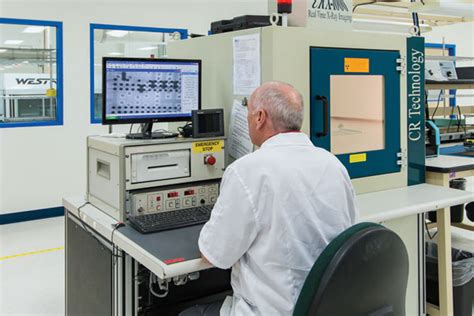
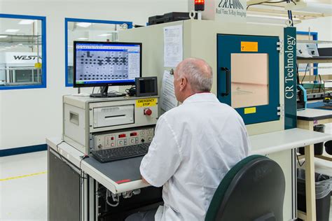
Modern PCB assembly processes increasingly rely on AI-driven systems to ensure zero-defect outcomes in high-volume production. By integrating machine learning algorithms with advanced optical inspection tools, manufacturers can detect microscopic solder joint anomalies, component misalignments, and substrate flaws at speeds exceeding 25,000 inspections per hour. These systems analyze historical PCBA data to predict failure patterns, enabling real-time adjustments to reflow profiles or pick-and-place machine calibration.
"AI-powered quality control reduces human error by 68% in SMT workflows, according to IPC-9151D benchmarking studies."
For industries like automotive electronics, where reliability standards demand near-perfect yields, AI models trained on AEC-Q100-compliant datasets validate thermal cycling resilience and vibration resistance during PCB assembly. Additionally, adaptive neural networks optimize material utilization by correlating solder paste deposition metrics with X-ray inspection results, minimizing waste while maintaining ISO 9001:2015 compliance.
As component miniaturization accelerates—particularly in IoT devices—AI systems now resolve challenges like 01005 package placement accuracy and microvia integrity verification. This technological synergy between SMT assembly and artificial intelligence not only elevates quality benchmarks but also aligns with Industry 4.0’s demand for self-optimizing manufacturing ecosystems.
Miniaturized Components in Modern SMT Tech
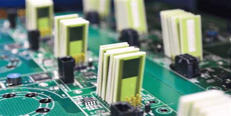
The relentless demand for compact, high-performance electronics has driven PCB assembly processes to adapt to increasingly miniaturized components. As devices shrink—from wearables to advanced medical implants—surface-mount technology (SMT) must accommodate components like 01005 passives (0.4mm x 0.2mm) and ultra-fine-pitch ICs with pitches below 0.3mm. Modern PCBA workflows leverage precision stencil printing and advanced pick-and-place systems capable of handling sub-millimeter tolerances, ensuring reliable placement of micro-scale resistors, capacitors, and chip-scale packages (CSPs).
However, miniaturization introduces challenges. Component warpage, solder bridging, and tombstoning become critical risks, necessitating AI-driven inspection systems to detect micron-level defects. Material science innovations, such as low-temperature co-fired ceramics (LTCC) and high-density interconnect (HDI) substrates, further support dense component layouts while maintaining thermal and electrical integrity. For industries like automotive and IoT, where space constraints coexist with harsh operating conditions, robust PCB assembly standards ensure miniaturized designs meet rigorous reliability requirements.
This evolution aligns with broader trends in PCBA, where component shrinkage enables smarter, lighter devices without compromising functionality. As SMT advances, the synergy between miniaturized components and precision manufacturing continues to redefine the boundaries of modern electronics.
SMT Solutions for IoT Electronics Production
The rapid proliferation of IoT devices demands SMT assembly processes capable of handling high-mix, low-volume production with uncompromising reliability. Modern PCB assembly lines optimized for IoT applications integrate ultra-precise pick-and-place systems to manage 0201 metric components and chip-scale packages (CSPs), ensuring compatibility with space-constrained wearables and sensor nodes. Advanced PCBA workflows now leverage real-time process monitoring to maintain yield rates above 99.95%, critical for IoT deployments in harsh industrial or environmental conditions.
To address these challenges, manufacturers deploy adaptive stencil printing and nitrogen-reflow soldering techniques, minimizing voiding in micro-BGA joints while accommodating flexible PCB substrates common in smart home and medical IoT devices. The integration of AI-driven optical inspection (AOI) aligns with IoT’s zero-defect requirements, detecting solder bridging or misalignments at resolutions below 10µm. For mission-critical applications like asset tracking systems, automated component verification ensures traceability from tape-and-reel sourcing to final assembly—a necessity for compliance with ISO 13485 and IEC 62443 standards.
This technological synergy between high-density interconnect (HDI) PCBA and IoT-specific design rules enables scalable production of energy-efficient edge-computing modules while maintaining <0.01% ppm defect rates. As 5G and LPWAN networks expand, these SMT solutions form the backbone of next-generation IoT ecosystems, balancing miniaturization with thermal management for extended operational lifespans.
Automotive-Grade SMT Assembly Standards
The automotive industry demands PCB assembly processes that exceed conventional reliability thresholds, requiring adherence to stringent AEC-Q100 and IPC Class 3 standards. Automotive-grade PCBA must withstand extreme temperatures, mechanical stress, and prolonged operational cycles, necessitating specialized SMT assembly protocols. Manufacturers employ high-temperature laminates, automotive-qualified components, and advanced soldering techniques like vacuum reflow to mitigate voiding in solder joints—a critical factor for electrical stability in harsh environments.
To ensure compliance, automated optical inspection (AOI) systems are calibrated to detect micron-level defects, while AI-driven quality control tools analyze thermal profiles and component placement accuracy in real time. These systems align with ISO 26262 functional safety requirements, verifying that every PCB assembly meets zero-failure benchmarks for applications like ADAS modules and powertrain controllers. Additionally, underfill encapsulation and conformal coating processes are optimized to protect against moisture ingress and vibration—key challenges in automotive electronics.
By integrating miniaturized components with automotive-specific SMT solutions, manufacturers achieve tighter trace spacing and higher component density without compromising durability. This precision supports the industry’s shift toward electric vehicles and connected systems, where reliability directly correlates with safety and performance. Transitioning to these standards ensures seamless compatibility with next-gen automotive PCBA architectures while maintaining scalability for high-volume production.
Industrial Electronics and SMT Innovations
The integration of SMT assembly services into industrial electronics manufacturing addresses the sector’s demand for robust, high-performance PCB assembly solutions. As industrial systems increasingly rely on automation controllers, power distribution modules, and sensor networks, PCBA processes must accommodate larger board formats, extended temperature tolerances, and enhanced vibration resistance. Advanced solder paste formulations with high-reliability alloys (e.g., SAC307) now enable consistent joint integrity in harsh environments, while vision-guided placement systems achieve ±15µm accuracy for high-power components like IGBT modules.
Building on automotive-grade SMT assembly standards, industrial applications benefit from conformal coating technologies that protect boards against moisture, dust, and chemical exposure. Manufacturers are adopting 3D AOI (Automated Optical Inspection) systems with machine learning algorithms to detect micro-cracks in through-hole connectors and surface-mount fuses. This synergy between PCB assembly precision and industrial durability ensures compliance with IEC 61131-2 for programmable logic controllers and UL 508A for industrial control panels.
The shift toward Industry 4.0 further drives innovations in PCBA traceability, with encrypted QR codes laser-etched onto substrates to track thermal cycling performance across a product’s lifecycle. These developments position SMT assembly services as critical enablers for next-generation industrial robotics, grid infrastructure, and predictive maintenance systems.
Optimizing PCB Manufacturing with SMT
Modern PCB assembly processes achieve unprecedented efficiency through surface-mount technology (SMT) advancements. By integrating precision automation and high-speed placement systems, SMT assembly services enable the production of complex PCBA designs with micron-level accuracy, reducing manual intervention and error rates. This optimization is critical for applications requiring miniaturized components, such as IoT sensors or automotive control modules, where component density directly impacts performance.
The shift to SMT-driven PCB manufacturing also enhances scalability. Automated optical inspection (AOI) systems paired with AI-driven analytics ensure consistent quality across high-volume production runs, while advanced solder paste printing techniques minimize defects in fine-pitch ICs. For industrial electronics, this translates to robust PCBA solutions capable of withstanding harsh environments. Additionally, SMT’s compatibility with mixed-technology boards allows seamless integration of through-hole and surface-mount components, future-proofing designs against evolving industry demands.
By leveraging SMT’s thermal management capabilities and material adaptability, manufacturers optimize heat dissipation in power electronics—a critical factor for automotive and aerospace applications. This technological synergy between PCB assembly workflows and SMT innovations ensures faster time-to-market and cost-efficiency without compromising reliability.
Future Trends in SMT Assembly Technology
The evolution of SMT assembly technology is accelerating to meet demands for higher-density, smarter, and more reliable PCBA solutions. A key trend centers on additive manufacturing techniques, enabling the integration of 3D-printed circuitry directly into PCB assembly workflows. This innovation reduces material waste while supporting complex geometries required for next-gen IoT and wearable devices. Additionally, advancements in hybrid electronics are blurring the lines between rigid and flexible substrates, empowering manufacturers to design compact, multi-functional boards for automotive and industrial systems.
Another transformative shift involves the adoption of AI-driven analytics for real-time process optimization. Machine learning algorithms now predict solder joint defects with 99.5% accuracy, minimizing rework in high-volume PCBA production. The rise of 5G-enabled edge computing further drives the need for ultra-miniaturized components, pushing SMT assembly toward sub-20-micron placement tolerances. Sustainability is also reshaping the sector, with biodegradable solder pastes and lead-free alloys gaining traction to comply with global environmental regulations.
As industries push toward Industry 4.0, digital twin simulations are becoming integral to PCB assembly lines, allowing virtual testing of thermal and mechanical stresses before physical production. These trends collectively position SMT technology as a cornerstone for advancing smart manufacturing ecosystems across automotive, aerospace, and consumer electronics sectors.
Conclusion
The evolution of SMT assembly technologies has redefined modern PCB manufacturing, offering unprecedented precision and scalability for industries ranging from IoT to automotive electronics. As PCBA processes integrate AI-driven quality control and ultra-miniaturized components, manufacturers achieve higher yields while meeting stringent reliability standards. These advancements not only address the growing complexity of circuit designs but also enable faster time-to-market for cutting-edge devices.
Looking ahead, the synergy between automated SMT workflows and smart factory ecosystems will further optimize PCB assembly efficiency, particularly for high-mix, low-volume production scenarios. Innovations in thermal management and material science continue to push the boundaries of what’s achievable in PCBA, ensuring compatibility with next-generation applications like 5G infrastructure and autonomous systems. By adopting these transformative solutions, electronics producers can maintain competitive agility while upholding the rigorous demands of today’s interconnected, data-driven markets.
FAQs
How does SMT technology improve efficiency in PCB assembly?
SMT assembly services enable high-speed placement of miniature components directly onto PCBA boards, reducing manual errors and increasing throughput. Automated optical inspection (AOI) systems paired with AI-driven quality control ensure defects are identified at sub-micron levels, critical for applications like IoT devices and automotive electronics.
What certifications are required for automotive-grade SMT assembly?
Automotive PCBA production demands compliance with ISO/TS 16949 and AEC-Q100 standards. These ensure components withstand extreme temperatures, vibrations, and humidity. Advanced SMT solutions incorporate 3D solder paste inspection and thermal cycling tests to meet rigorous reliability requirements.
Can miniaturized components affect PCB manufacturing yields?
While components like 01005 chips pose placement challenges, modern SMT assembly services leverage precision nozzles and vision-guided robotics to achieve placement accuracy within ±25µm. Enhanced reflow profiling further minimizes solder bridging, maintaining yields above 99.5% for complex PCBA designs.
How is AI integrated into SMT quality control processes?
Machine learning algorithms analyze real-time data from X-ray inspection and AOI systems, detecting anomalies such as tombstoning or insufficient solder. This predictive maintenance approach reduces downtime by 30% and improves defect detection rates to 99.9% in high-mix PCB assembly environments.
What innovations are shaping industrial electronics SMT workflows?
Emerging trends include laser-assisted soldering for heat-sensitive components and digital twin simulations to optimize PCBA layouts. These advancements support faster prototyping and ensure compatibility with Industry 4.0 automation standards.
Ready to Optimize Your PCB Production?
Explore our cutting-edge SMT assembly services tailored for automotive, IoT, and industrial applications. Click here to discover how we enhance your PCB manufacturing workflows.