Advanced SMT PCBA Manufacturing Solutions for Next-Gen Electronics

Key Takeaways
Modern SMT PCBA manufacturing is foundational to next-generation electronics, enabling innovations in IoT, AI, and 5G applications. By leveraging automated assembly techniques, manufacturers achieve micron-level precision in PCB assembly, critical for high-density designs. Advanced surface-mount technology (SMT) processes ensure consistent solder joint quality, reducing defects by up to 40% compared to traditional methods.
A key advantage lies in scalable PCBA solutions, which support rapid prototyping and mass production for 5G infrastructure. For example, automated optical inspection (AOI) systems paired with X-ray testing validate component alignment and solder integrity, aligning with ISO 9001 and IPC-A-610 standards.
| Parameter | Traditional PCBA | Advanced SMT PCBA |
|---|---|---|
| Placement Accuracy | ±50µm | ±15µm |
| Defect Rate | 500 ppm | <100 ppm |
| Throughput (units/hr) | 8,000 | 25,000 |
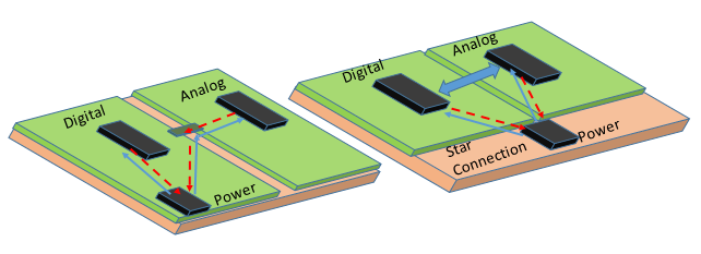
Rigorous quality controls, including in-circuit testing (ICT) and functional testing, ensure high-reliability electronics for mission-critical systems. Manufacturers like QualiEco Circuits integrate AI-driven process optimization to minimize thermal stress during reflow soldering, enhancing product longevity. Crucially, high-density interconnect (HDI) PCBA techniques enable compact, power-efficient designs demanded by AI accelerators and edge-computing devices. These advancements underscore the shift toward smart manufacturing ecosystems, where real-time data analytics drive continuous improvement in SMT PCBA production.

SMT PCBA Innovations for IoT and AI Devices
The rapid evolution of IoT and AI technologies demands PCB assembly processes that balance miniaturization with high-speed performance. Modern SMT PCBA systems now integrate advanced pick-and-place robotics, enabling precise mounting of ultra-fine-pitch components like micro-BGA packages and 01005 passives. These innovations are critical for devices requiring high-density interconnects, such as edge-computing modules and AI accelerators. For instance, automated optical inspection (AOI) systems paired with AI-driven defect detection algorithms ensure sub-10μm alignment accuracy, reducing rework rates by up to 40% in mission-critical applications.
To address thermal management challenges in compact IoT hardware, manufacturers are adopting low-loss dielectric materials and laser-drilled microvias within PCBA layers. This enhances signal integrity while dissipating heat from power-hungry AI chipsets. Additionally, hybrid soldering techniques combining conductive adhesives with lead-free alloys improve reliability in harsh environments, such as industrial IoT sensors operating at extreme temperatures.
Scalability remains a cornerstone of SMT PCBA innovation, with modular production lines supporting rapid transitions between low-volume prototyping and high-mix manufacturing. This flexibility aligns with the iterative design cycles of 5G-enabled AI devices, where optimized assembly workflows minimize time-to-market without compromising on electromagnetic compatibility (EMC) standards. As IoT and AI applications expand, advancements in PCB assembly will continue to prioritize energy efficiency, signal speed, and lifecycle durability.
Automated Assembly Techniques in PCBA Manufacturing
Modern PCB assembly processes rely heavily on automation to meet the precision and speed demands of next-generation electronics. PCBA production lines now integrate robotic pick-and-place systems, which achieve component placement accuracy within ±25 microns, critical for high-density interconnect (HDI) designs. Advanced vision systems paired with machine learning algorithms ensure real-time error detection, minimizing defects in SMT-driven workflows.
Tip: For IoT and AI hardware, consider modular automation platforms that allow rapid reconfiguration to accommodate varying component sizes and board geometries.
Automated solder paste dispensers and reflow ovens further enhance consistency, particularly for fine-pitch components like 0.4mm BGA packages. Closed-loop feedback mechanisms adjust parameters such as temperature profiles and conveyor speeds, optimizing yield rates. Collaborative robots (cobots) are increasingly deployed for tasks like post-assembly inspection, working alongside human operators to balance efficiency and precision.
Transitioning to lights-out manufacturing models, some facilities now operate with minimal human intervention, leveraging IoT-enabled machinery for predictive maintenance. This shift not only reduces cycle times but also ensures traceability across PCBA batches, a necessity for industries like 5G infrastructure and medical devices. By combining PCB assembly automation with data analytics, manufacturers achieve scalable production while maintaining compliance with ISO 9001 and IPC-A-610 standards.

Enhancing Electronics Reliability Through SMT Processes
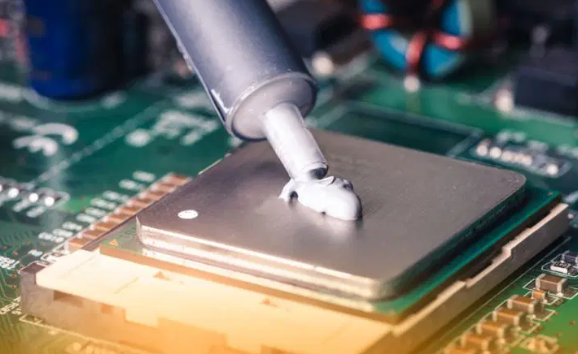
Modern PCB assembly relies on surface-mount technology (SMT) to address critical challenges in electronic reliability. By optimizing solder paste application, component placement accuracy, and reflow profiling, manufacturers achieve consistent electrical connectivity and reduced failure rates in PCBA for high-stress environments. Automated optical inspection (AOI) systems, such as those developed by Omron, ensure micron-level defect detection, minimizing risks like tombstoning or solder bridging.
Advanced SMT processes also enhance thermal management through precision-controlled reflow ovens and thermally stable substrates, which mitigate stress-induced fractures in components. For mission-critical applications—such as aerospace or medical devices—PCBA workflows integrate in-situ testing and environmental stress screening (ESS) to validate long-term performance under extreme conditions. This approach not only reduces field failures but also aligns with ISO 9001 and IPC-A-610 standards, reinforcing trust in next-generation electronics.
As IoT and 5G systems demand higher component densities, SMT innovations like laser-direct imaging (LDI) and conductive epoxy adhesives enable robust interconnects even in miniaturized designs. By balancing speed and precision, manufacturers deliver PCB assembly solutions that prioritize reliability without compromising scalability for emerging technologies.
Scalable SMT Solutions for 5G Hardware Production
The rapid deployment of 5G networks demands scalable SMT solutions capable of supporting high-frequency, low-latency hardware requirements. Modern PCB assembly processes leverage automated pick-and-place systems and ultra-precision solder paste printing to handle millimeter-wave circuitry and miniaturized components essential for 5G base stations and edge devices. By integrating PCBA workflows with AI-driven process optimization, manufacturers achieve yield rates exceeding 99.2% even when assembling high-density boards with 01005 passives or 0.4mm-pitch BGAs.
For 5G-specific applications, advanced SMT production lines now incorporate in-line 3D AOI and X-ray inspection to validate signal integrity in RF modules and antenna arrays. This is critical as 5G hardware operates at frequencies up to 39GHz, where even micron-level soldering defects can degrade performance. Scalability is further enhanced through modular PCB assembly platforms, allowing seamless transitions between prototyping and mass production without compromising thermal management or EMI shielding standards.
Leading manufacturers are adopting adaptive stencil technologies and nitrogen-reflow environments to stabilize PCBA outcomes across varying batch sizes. These strategies ensure consistent impedance control in multi-layer FR4 and Rogers substrates, directly addressing 5G’s demand for ultra-low loss interconnects. As global 5G adoption accelerates, vertically integrated PCB assembly ecosystems remain pivotal in balancing cost-efficiency with the stringent reliability requirements of next-generation wireless infrastructure.
Precision-Driven PCBA Manufacturing Best Practices
Achieving micron-level accuracy in PCBA production requires harmonizing advanced equipment with stringent process controls. Modern high-density interconnect (HDI) designs demand precise solder paste deposition, typically using stencils with apertures under 100µm, paired with automated optical inspection (AOI) systems to detect sub-25µm defects. For mission-critical applications like medical IoT or aerospace systems, thermal profiling ensures consistent reflow soldering, mitigating risks like PCB warpage during thermal cycling.
Leading manufacturers integrate PCB assembly workflows with machine learning algorithms to optimize component placement accuracy, reducing misalignment by over 40% in complex layouts. Real-time data analytics further refine processes, such as adjusting pick-and-place speed for delicate components like 01005 resistors or ultra-fine-pitch BGAs. Rigorous material selection—including low-temperature co-fired ceramics (LTCC) for 5G RF modules—minimizes signal loss in high-frequency applications.
To maintain consistency, inline X-ray inspection (AXI) validates solder joint integrity, particularly for hidden connections in multilayer boards. By aligning these practices with ISO 9001 and IPC-A-610 standards, manufacturers ensure scalable precision across prototypes and high-volume runs, directly supporting next-gen electronics’ reliability and performance thresholds.
Quality Control Standards in Advanced SMT Assembly
Modern PCB assembly processes demand rigorous quality control to meet the performance requirements of next-generation electronics. In SMT PCBA manufacturing, automated optical inspection (AOI) systems and X-ray testing are critical for detecting solder joint defects, component misalignment, and hidden faults in high-density designs. Advanced systems now leverage machine learning algorithms to improve defect recognition accuracy, reducing false positives by up to 30% compared to traditional methods.
Compliance with international standards like IPC-A-610 and ISO 9001:2015 ensures consistency across production batches, particularly for mission-critical applications in 5G infrastructure and AI hardware. For instance, solder void analysis has become a focal point, with leading manufacturers maintaining void rates below 5% to optimize thermal management in compact PCBA designs. Real-time process monitoring tools further validate parameters such as reflow oven temperature profiles and paste deposition accuracy, preventing deviations that could compromise long-term reliability.
Material traceability systems are equally vital, tracking components from procurement to final assembly to mitigate counterfeit risks. By integrating these protocols, SMT PCBA providers achieve defect rates under 50 parts per million (PPM), ensuring scalability for IoT and edge-computing devices requiring zero-failure operation. This multi-layered approach not only aligns with industry benchmarks but also adapts dynamically to evolving technological demands.

Optimizing High-Density PCBA for Next-Gen Tech
As next-generation electronics demand smaller footprints and higher functionality, optimizing high-density PCBA becomes critical for IoT, AI, and 5G applications. Modern PCB assembly processes now prioritize miniaturization and signal integrity to accommodate densely packed components like micro-BGAs and ultra-fine-pitch ICs. Advanced SMT techniques, including laser-direct imaging and precision solder paste deposition, enable tighter tolerances for traces and vias, reducing electromagnetic interference (EMI) in PCBA designs.
To address thermal challenges in high-density layouts, engineers employ embedded cooling solutions and thermally conductive substrates. These innovations ensure stable performance in compact devices operating under extreme loads. Additionally, automated optical inspection (AOI) and 3D X-ray systems rigorously validate solder joint quality, minimizing defects in multilayer PCB assembly.
Scalability remains a key focus, with modular production lines integrating adaptive pick-and-place systems and AI-driven process control. This flexibility supports rapid transitions between prototypes and mass production, essential for evolving 5G infrastructure and edge-computing hardware. By balancing design complexity with manufacturability, optimized PCBA workflows deliver reliability without compromising speed—a cornerstone for next-gen electronics innovation.
Smart Manufacturing Trends in SMT PCBA Systems
The evolution of PCB assembly processes is increasingly defined by smart manufacturing principles, particularly in SMT PCBA systems. Modern facilities now integrate IoT-enabled monitoring and AI-driven analytics to optimize production workflows, reducing defects and improving throughput. Real-time data collection from PCBA lines enables predictive maintenance, minimizing downtime caused by equipment failures. Advanced vision systems paired with machine learning algorithms enhance component placement accuracy, critical for high-density boards used in 5G infrastructure and AI hardware.
Another key trend is the adoption of digital twin technology, which creates virtual replicas of PCB assembly lines to simulate and refine processes before physical implementation. This reduces trial-and-error cycles and accelerates time-to-market for complex electronics. Additionally, modular SMT PCBA systems allow manufacturers to reconfigure production lines swiftly, supporting flexible scaling for fluctuating demand in IoT device markets.
Energy-efficient practices are also gaining traction, with smart sensors optimizing power consumption during PCBA soldering and testing phases. These innovations align with Industry 4.0 standards, ensuring seamless interoperability between machinery and enterprise resource planning (ERP) systems. By embracing these trends, manufacturers achieve tighter process control while maintaining compliance with evolving quality benchmarks for next-generation electronics.
Conclusion
The evolution of SMT PCBA manufacturing underscores its indispensable role in powering next-generation electronics, from AI-driven systems to 5G infrastructure. By integrating automated assembly processes and precision-driven workflows, manufacturers achieve unparalleled consistency in PCB assembly, ensuring high yields even for complex, miniaturized designs. Advanced PCBA solutions now prioritize scalability and reliability, leveraging smart inspection systems and high-density interconnect (HDI) techniques to meet the demands of IoT and edge computing devices.
Rigorous quality control protocols, including automated optical inspection (AOI) and X-ray testing, mitigate risks in mission-critical applications, while modular production lines enable rapid adaptation to evolving 5G hardware standards. As industries embrace smart manufacturing trends, the synergy between SMT processes and data-driven analytics optimizes throughput without compromising precision soldering or thermal management.
Ultimately, the success of modern electronics hinges on holistic innovation in PCBA manufacturing—balancing speed, accuracy, and sustainability. By adopting these advanced methodologies, manufacturers position themselves at the forefront of a rapidly transforming technological landscape.
FAQs
How does SMT technology improve efficiency in PCB assembly for IoT devices?
SMT (Surface Mount Technology) enables high-speed placement of miniature components, critical for compact IoT designs. Automated pick-and-place systems ensure precise alignment, reducing manual errors and accelerating PCBA production cycles.
What quality controls are essential for high-density PCBA in AI hardware?
Advanced PCB assembly processes integrate automated optical inspection (AOI) and X-ray testing to detect solder joint defects or component misalignments. These steps ensure reliability in AI systems, where even minor flaws can disrupt performance.
Can SMT solutions scale for 5G infrastructure demands?
Yes. Modular PCBA lines with flexible reflow soldering profiles support rapid scaling. Manufacturers optimize thermal management and signal integrity to meet 5G’s high-frequency requirements while maintaining throughput.
Why is precision critical in PCB assembly for medical electronics?
Medical devices demand near-zero defect rates. SMT processes leverage laser-cut stencils and nitrogen-reflow environments to achieve micron-level accuracy, ensuring compliance with stringent industry standards.
How do smart manufacturing trends impact PCBA costs?
IoT-enabled predictive maintenance and digital twins reduce downtime and material waste. Real-time monitoring of PCB assembly lines cuts operational costs by up to 20%, benefiting high-volume production.
Ready to Optimize Your Next-Gen Electronics Production?
For tailored SMT PCBA solutions that align with your project’s technical demands, please click here to explore advanced manufacturing capabilities.