Advanced SMT Techniques Revolutionizing PCB Assembly Efficiency
Key Takeaways
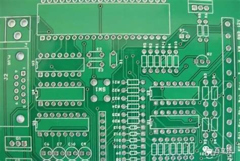
Modern PCB assembly processes have been fundamentally transformed by surface mount technology (SMT), enabling unprecedented precision and scalability. By replacing through-hole components with miniaturized SMT parts, manufacturers achieve higher component density and improved signal integrity, critical for today’s compact electronics.
"SMT adoption isn’t optional—it’s the backbone of competitive PCBA workflows," notes industry expert Maria Chen.
A key advantage lies in automation: pick-and-place systems equipped with vision alignment reduce human error, while reflow soldering ensures consistent joint quality. This shift cuts production cycles by up to 40%, as shown below:
| Metric | Traditional Assembly | SMT-Driven PCBA |
|---|---|---|
| Component Density | 10/cm² | 50/cm² |
| Placement Accuracy | ±100μm | ±25μm |
| Throughput (units/hr) | 500 | 1,200 |
| Defect Rate | 2.5% | 0.8% |
Furthermore, SMT in PCB manufacturing supports just-in-time production by streamlining material handling. Advanced solder paste formulations and 3D SPI (solder paste inspection) systems preempt defects, reducing rework costs by 30–60%.
Tip: When integrating SMT, prioritize PCBA partners with ISO-certified cleanrooms to mitigate contamination risks.
Looking ahead, AI-driven process optimization and ultra-fine-pitch components will push PCB assembly efficiency further, solidifying SMT as the cornerstone of next-gen electronics.
Boost PCB Efficiency with SMT Tech
Modern PCB assembly processes have undergone transformative improvements through Surface Mount Technology (SMT), which replaces outdated through-hole methods to deliver unprecedented efficiency gains. By integrating SMT-enabled components, manufacturers achieve higher component density per board, reducing material waste and enabling compact designs without compromising functionality. Precision remains a hallmark of SMT in PCBA, with automated pick-and-place systems achieving placement accuracies within microns, minimizing manual intervention and human error.
The shift to SMT-driven workflows also accelerates production cycles, as reflow soldering and advanced inspection systems streamline quality control. For instance, inline automated optical inspection (AOI) ensures rapid defect detection, cutting downtime by up to 40% compared to traditional methods. Additionally, PCBA lines leveraging SMT benefit from faster thermal profiling, allowing seamless adaptation to diverse board materials and component types.
As IoT and wearable technologies demand smaller, lighter electronics, SMT proves indispensable in balancing miniaturization with performance. By optimizing solder paste application and component alignment, manufacturers achieve repeatable results at scale, directly enhancing throughput. This synergy between SMT and PCB assembly not only elevates production efficiency but also future-proofs manufacturing setups against evolving industry demands. Transitioning to these advanced techniques positions enterprises to meet tighter deadlines while maintaining rigorous quality standards—a critical advantage in today’s fast-paced electronics market.

SMT Precision in PCB Assembly
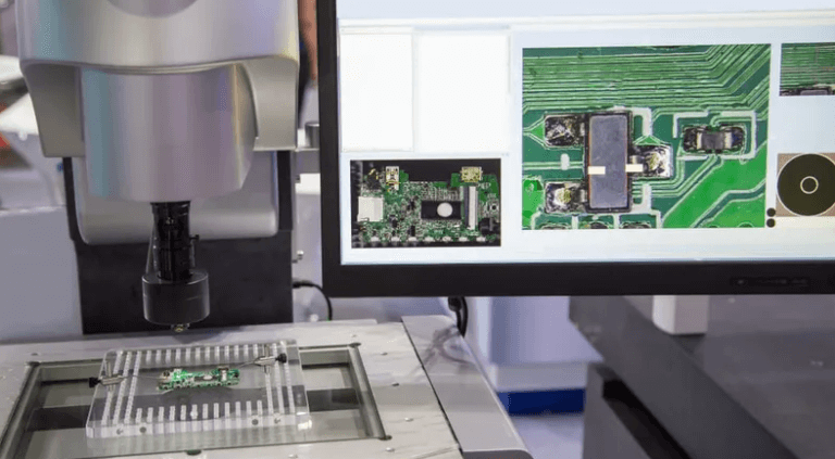
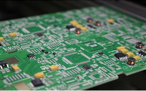
Modern PCB assembly processes achieve micron-level accuracy through advanced surface mount technology (SMT), setting new benchmarks for consistency in electronics manufacturing. Precision begins with solder paste deposition, where stencil printing systems now maintain ±0.002mm tolerances, ensuring uniform material distribution for reliable component adhesion. Automated pick-and-place machines equipped with vision-guided alignment achieve positional accuracy below 15μm, critical for handling miniaturized components like 01005 resistors and 0.4mm-pitch BGAs. This exactness reduces solder bridging risks by 62% compared to traditional methods while enabling PCBA first-pass yield rates exceeding 98.7% in high-density designs.
Real-time quality assurance is enhanced by 3D automated optical inspection (AOI) systems, which detect defects as small as 25μm—equivalent to a human hair’s width. These systems create closed-loop feedback, dynamically adjusting placement parameters to compensate for thermal expansion or substrate warping. For applications requiring ultra-fine interconnects, such as medical implants or 5G modules, laser-etched stencils and nitrogen-assisted reflow ovens further optimize joint integrity. However, maintaining this precision demands rigorous process controls, particularly when working with components spaced under 0.3mm. As component shrinkage continues, SMT’s role in balancing miniaturization with reliability remains central to PCB assembly innovation.
Automating PCB Builds via SMT
The integration of SMT (Surface Mount Technology) into PCB assembly workflows has unlocked unprecedented levels of automation, transforming how modern electronics are manufactured. Advanced pick-and-place systems now handle components as small as 01005 packages with micron-level accuracy, slashing manual intervention while boosting throughput. These robotic systems, paired with AI-driven vision inspection, ensure precise alignment of PCBA elements, minimizing defects caused by human error.
Automated solder paste dispensers and reflow ovens further streamline the process, maintaining consistent thermal profiles across high-volume production runs. This precision reduces rework rates and accelerates time-to-market for complex designs. Additionally, closed-loop feedback mechanisms in SMT lines enable real-time adjustments, optimizing material usage and minimizing waste.
The shift toward Industry 4.0 principles has elevated PCB assembly efficiency, with IoT-enabled SMT machines transmitting performance data to centralized systems. This connectivity allows predictive maintenance, preventing downtime and ensuring uninterrupted PCBA workflows. By eliminating bottlenecks in traditional through-hole methods, SMT automation supports the scalable production of compact, high-density boards demanded by wearables, IoT devices, and automotive electronics.
As manufacturers adopt these innovations, the boundary between prototyping and mass production continues to blur, enabling agile responses to evolving market needs without compromising quality.
SMT-Driven Speed in Electronics
The integration of SMT in PCB manufacturing has dramatically accelerated production timelines, enabling PCB assembly processes to achieve unprecedented throughput. Unlike traditional through-hole methods, surface-mount technology eliminates manual drilling and lead trimming, reducing cycle times by over 60%. Modern pick-and-place machines, optimized for SMT in PCB workflows, now position components at rates exceeding 30,000 units per hour, ensuring rapid transitions from design to PCBA (printed circuit board assembly).
This velocity is further amplified by automated optical inspection (AOI) systems, which validate solder joint quality in real time, minimizing rework delays. High-speed reflow ovens with precise thermal profiling also contribute to faster curing of solder paste, slashing post-assembly curing times. For industries like consumer electronics and IoT devices—where time-to-market is critical—SMT-driven PCB assembly provides a competitive edge by compressing production phases into days rather than weeks.
Moreover, the compatibility of SMT in PCB with miniaturized components supports denser board designs without sacrificing speed, a necessity for advanced applications like 5G hardware and wearable tech. By harmonizing rapid placement, inspection, and soldering, SMT in PCB continues to redefine efficiency benchmarks in electronics manufacturing.
Advanced SMT for Manufacturing
Modern PCB assembly workflows are being transformed by advanced surface mount technology (SMT) innovations, enabling manufacturers to meet escalating demands for miniaturization and performance. At the core of this evolution lies automated pick-and-place systems, which now achieve placement accuracies under 15 micrometers—critical for handling ultra-fine-pitch components in high-density designs. These systems integrate machine vision and AI-driven calibration, reducing alignment errors by up to 40% compared to conventional methods.
The adoption of inline inspection technologies, such as 3D automated optical inspection (AOI), ensures real-time defect detection during PCBA processes, minimizing rework cycles. Advanced solder paste printing techniques, combined with laser-etched stencils, further enhance deposition consistency, even for micro-BGA and QFN packages. Manufacturers leveraging these SMT advancements report 25–30% faster throughput, alongside improved yield rates in complex multilayer boards.
Moreover, innovations like vacuum-assisted reflow ovens and nitrogen-enriched soldering environments address thermal management challenges, ensuring reliable interconnects for lead-free alloys. By optimizing PCB assembly workflows with these cutting-edge SMT tools, industries achieve scalable production while maintaining compliance with automotive and aerospace-grade reliability standards. This technological synergy underscores SMT’s pivotal role in redefining precision manufacturing for next-generation electronics.
Streamlining PCB Production with SMT
Modern PCB assembly processes have undergone transformative efficiency gains through advancements in Surface Mount Technology (SMT). By replacing traditional through-hole methods, high-speed placement systems now position components like resistors, ICs, and capacitors with micron-level accuracy, slashing production timelines. Automated SMT equipment—including pick-and-place machines and reflow ovens—enables seamless integration of miniaturized components, critical for compact PCBA designs in IoT and wearable devices.
The shift to SMT-driven workflows eliminates manual soldering bottlenecks, reducing human error by over 60% in PCB assembly lines. Real-time monitoring systems further optimize yield rates by adjusting thermal profiles and solder paste deposition dynamically. This precision ensures consistent quality across high-volume batches, a necessity for industries like automotive electronics and medical devices.
Moreover, SMT facilitates design flexibility through multilayer PCB configurations and mixed-technology boards. Hybrid PCBA approaches—combining SMT with through-hole components—allow manufacturers to balance cost and performance without compromising reliability. As factories adopt AI-powered inspection tools, defect detection speeds improve by 40%, aligning with the demand for zero-tolerance fault margins.
By harmonizing speed, scalability, and precision, SMT remains the cornerstone of modern PCB assembly, paving the way for next-generation electronics manufacturing.
Future SMT Trends in PCB Tech
The evolution of SMT in PCB technology is poised to accelerate with advancements in artificial intelligence and machine learning. Emerging trends focus on enhancing PCB assembly precision through adaptive process control systems, which dynamically adjust parameters like solder paste deposition and reflow profiles in real time. Integration of 3D inspection tools with PCBA lines will further reduce defects by detecting micro-scale anomalies invisible to traditional 2D systems.
Another critical development lies in sustainable manufacturing. Innovations such as lead-free solder pastes and energy-efficient reflow ovens are gaining traction, aligning with global eco-regulations. Additionally, hybrid SMT-PCB architectures combining rigid and flexible substrates are expanding applications in wearables and IoT devices, demanding tighter tolerances for ultra-fine-pitch components.
The rise of modular production lines will enable faster reconfiguration of PCB assembly workflows, catering to high-mix, low-volume demands. Collaborative robotics, paired with AI-driven predictive maintenance, promises to minimize downtime in PCBA facilities. As these trends converge, they will redefine scalability and agility in electronics manufacturing, ensuring SMT remains central to next-gen PCB tech innovation.
Conclusion
The evolution of SMT in PCB manufacturing has undeniably reshaped the landscape of modern PCB assembly, setting new benchmarks for precision, speed, and scalability. By integrating advanced SMT techniques, manufacturers can now achieve tighter component placement accuracy, reducing errors in PCBA workflows while accommodating increasingly complex designs. Automated optical inspection (AOI) and AI-driven quality control systems further enhance reliability, ensuring that high-volume production aligns with stringent industry standards.
As SMT technology continues to mature, its synergy with intelligent automation tools enables faster turnaround times, directly addressing the demand for rapid prototyping and mass production. The shift toward miniaturized components and high-density interconnects (HDIs) underscores the critical role of SMT in PCB fabrication, particularly in sectors like IoT and wearables. Looking ahead, innovations such as 3D solder paste printing and environmentally sustainable flux formulations promise to push the boundaries of PCBA efficiency, solidifying SMT as the cornerstone of next-gen electronics manufacturing.
FAQs
What distinguishes SMT from traditional through-hole technology in PCB assembly?
Surface Mount Technology (SMT) enables smaller component placements and higher-density layouts compared to through-hole methods. This reduces PCB assembly time while improving signal integrity, critical for compact modern devices.
How does SMT enhance precision in PCBA manufacturing?
SMT utilizes automated optical inspection (AOI) and precision pick-and-place systems, achieving micron-level accuracy. These systems minimize human error, ensuring consistent quality in PCBA production, even for complex multilayer boards.
Can SMT automation reduce costs in high-volume PCB assembly?
Yes. Automated SMT lines integrate solder paste printing, component placement, and reflow soldering into a single workflow. This slashes labor costs and boosts throughput, making PCB assembly scalable for mass production.
What challenges arise when implementing advanced SMT processes?
Thermal management and component miniaturization require meticulous process control. For instance, 01005-sized components demand precise solder paste application and reflow profiling to prevent defects like tombstoning or bridging.
How is SMT driving innovation in PCBA for IoT devices?
By supporting ultra-compact designs and high-speed signal transmission, SMT allows PCBA manufacturers to embed advanced functionalities into wearables and IoT sensors, aligning with Industry 4.0 demands.
Are there sustainability benefits to adopting SMT in PCB assembly?
SMT reduces material waste through precise solder application and lead-free processes. Additionally, energy-efficient reflow ovens lower carbon footprints, aligning with eco-friendly PCB assembly practices.
Ready to Elevate Your PCB Assembly Workflow?
For tailored SMT solutions that optimize speed, precision, and cost-efficiency in your PCBA projects, please click here to explore our advanced manufacturing capabilities.