Advanced Strategies for PCB Board Assembly Manufactur
Key Takeaway
Modern PCB assembly processes demand a strategic blend of automation and intelligent systems to achieve optimal outcomes. Central to this approach is the integration of automated workflows, which streamline PCBA production by minimizing human error and accelerating throughput. Advanced robotic systems now handle tasks like solder paste application and component placement with sub-micron precision, ensuring consistency across high-volume batches. Complementing this, smart sensors and IoT-enabled devices monitor real-time data—such as temperature fluctuations or vibration levels—to preemptively address deviations in quality control.
Cost-efficiency is further enhanced through AI-driven analytics, which optimize material usage and predict equipment maintenance needs, reducing downtime. For instance, machine learning algorithms analyze historical PCB manufacturing data to refine placement patterns, trimming waste by up to 15%. Meanwhile, modular production lines allow rapid reconfiguration for diverse PCBA designs, catering to both prototyping and mass production.
By harmonizing precision methods with adaptive technologies, manufacturers can balance scalability and customization without compromising reliability. This synergy not only elevates end-product performance but also positions firms to adapt swiftly to evolving industry standards and client demands.
Automated PCB Assembly Workflows
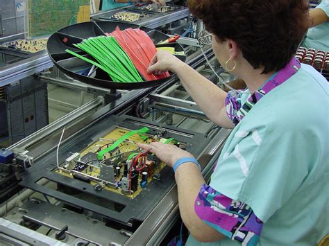
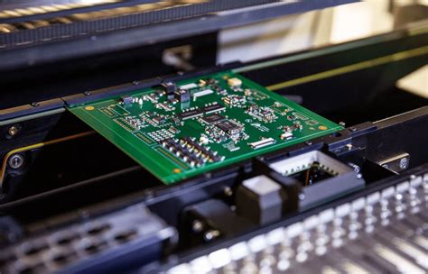
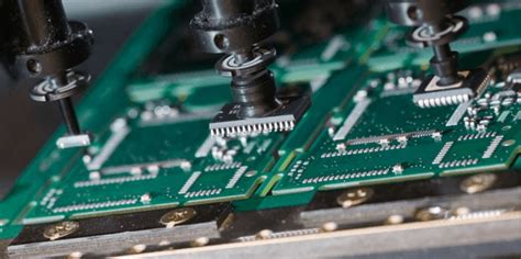
Modern PCB assembly processes have undergone transformative changes with the adoption of automated workflows. By integrating robotic systems, manufacturers achieve unprecedented precision in component placement, soldering, and inspection. For instance, PCBA (Printed Circuit Board Assembly) lines now leverage high-speed pick-and-place machines capable of positioning microcomponents at rates exceeding 25,000 placements per hour, minimizing human error while boosting throughput.
A critical advantage lies in the synchronization of automated optical inspection (AOI) systems with real-time data analytics. These systems identify defects such as solder bridging or misaligned components with sub-micron accuracy, ensuring compliance with industry standards like IPC-A-610. The table below highlights key metrics comparing manual and automated workflows:
| Metric | Manual Assembly | Automated Assembly |
|---|---|---|
| Throughput (units/hr) | 50–100 | 500–1,200 |
| Defect Rate | 0.5–1.2% | <0.1% |
| Scalability | Low | High |
To optimize PCB assembly workflows, manufacturers are adopting modular automation frameworks. These systems allow seamless reconfiguration for diverse product batches, reducing downtime by 40–60%. Additionally, closed-loop feedback mechanisms between AOI and solder paste printers enable self-correction of process parameters, enhancing yield rates.
The integration of PCBA automation with enterprise resource planning (ERP) software further streamlines material logistics, ensuring just-in-time component delivery. Emerging trends include machine learning algorithms that predict equipment maintenance needs, reducing unplanned outages by up to 30%. As industries demand smaller, more complex boards, automated workflows remain pivotal in balancing precision, speed, and cost-efficiency.
Smart Tech Integration in PCB Manufacturing
The integration of smart manufacturing systems into PCB assembly processes is reshaping production efficiency and accuracy. By embedding IoT-enabled sensors and AI-driven analytics into PCBA workflows, manufacturers gain real-time visibility into equipment performance, material usage, and defect rates. For instance, machine learning algorithms analyze historical production data to predict component placement errors, reducing rework by up to 30%.
Tip: Prioritize IoT platforms that support seamless integration with existing PCB assembly machinery to minimize downtime during tech upgrades.
Advanced PCBA lines now leverage digital twins—virtual replicas of physical production systems—to simulate and optimize processes before implementation. This approach cuts trial-and-error cycles while ensuring compatibility with high-density interconnect (HDI) designs. Additionally, automated optical inspection (AOI) systems equipped with AI-powered image recognition achieve defect detection rates exceeding 99.5%, far surpassing manual inspections.
Transitioning to smart factories also enables adaptive resource allocation. For example, cloud-based monitoring tools dynamically adjust solder paste application parameters based on real-time environmental data, ensuring consistent joint quality across batches. Such innovations not only streamline PCB assembly but also create a foundation for scalable, data-driven decision-making in complex manufacturing ecosystems.
Precision Methods for PCB Assembly
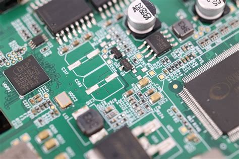
Achieving micron-level accuracy in PCB assembly requires a systematic integration of advanced technologies and rigorous process controls. Modern automated optical inspection (AOI) systems now deploy high-resolution cameras paired with machine learning algorithms to detect soldering defects as small as 15µm, ensuring PCBA outputs meet stringent industry standards. For critical applications like aerospace or medical devices, laser direct imaging (LDI) replaces traditional photolithography, enabling trace widths under 40µm with ±2µm positional accuracy.
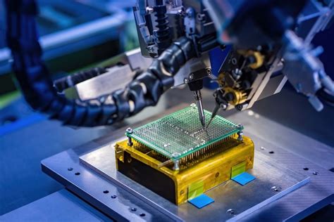
To minimize human error, factories increasingly adopt automated pick-and-place robots equipped with vision-guided alignment, achieving placement precision of 0.025mm for 01005-sized components. These systems work in tandem with solder paste inspection (SPI) tools that verify deposition volume within 5% tolerances, directly impacting PCB assembly reliability. Thermal profiling during reflow soldering has also evolved, with real-time closed-loop systems adjusting zone temperatures ±1°C to maintain optimal alloy flow across complex multilayer boards.
For high-density interconnect (HDI) PCBA, manufacturers implement X-ray inspection to validate hidden joints in ball grid arrays (BGAs), while in-circuit testing (ICT) fixtures verify electrical continuity at 10mV resolution. Such precision methods reduce defect rates to <50 parts per million (PPM) in tier-1 facilities, demonstrating how technological investments directly correlate with PCB assembly quality outcomes.
Quality Control in PCB Production
Effective PCB assembly processes rely on rigorous quality control protocols to ensure end-product reliability. Modern PCBA production integrates automated optical inspection (AOI) systems, which scan boards for soldering defects, component misalignment, and trace integrity at speeds exceeding 10,000 points per minute. These systems are complemented by statistical process control (SPC) methodologies, where real-time data from assembly lines identifies deviations in parameters like solder paste volume or reflow oven temperatures.
To maintain consistency, manufacturers employ cross-functional verification workflows, combining AOI with X-ray inspection for hidden faults in ball grid arrays (BGAs) and multilayer boards. Environmental controls further stabilize outcomes, with humidity and temperature-regulated cleanrooms preventing oxidation during PCB assembly. Advanced traceability systems, powered by QR codes or RFID tags, enable granular tracking of each batch, linking test results to specific production stages.
For PCBA projects requiring high-reliability certification (e.g., aerospace or medical devices), failure mode and effects analysis (FMEA) preemptively addresses risks, while in-circuit testing (ICT) validates electrical performance against design specifications. By aligning these strategies with ISO 9001 and IPC-A-610 standards, manufacturers minimize rework rates and uphold zero-defect objectives without compromising throughput.
Cost-Efficient PCB Manufacturing Strategies
Achieving cost efficiency in PCB assembly requires a strategic balance between process optimization and technology adoption. One proven approach involves implementing automated assembly lines to minimize manual labor costs while maintaining consistent output quality. By integrating PCBA-specific robotic pick-and-place systems, manufacturers can reduce component placement errors by up to 70%, directly lowering rework expenses.
Material procurement strategies also play a pivotal role—leveraging predictive analytics to optimize inventory levels prevents overstocking of high-cost substrates and solder pastes. Additionally, adopting design-for-manufacturability (DFM) principles early in the development phase ensures layouts are optimized for automated production, reducing material waste by 15–20%.
Smart factory technologies further enhance cost control through real-time energy monitoring and predictive maintenance systems. For instance, IoT-enabled sensors in PCB assembly equipment can preemptively flag calibration drifts, avoiding costly unplanned downtime. Bulk purchasing agreements with certified component suppliers, coupled with modular PCBA designs that allow for part substitutions during shortages, provide additional resilience against supply chain volatility.
By aligning these tactics with lean manufacturing frameworks, businesses achieve scalable cost reductions without compromising the precision required for complex multilayer boards—a critical advantage in competitive electronics markets.
Optimizing PCB Production Workflows
Streamlining PCB assembly workflows requires a holistic approach that balances speed, accuracy, and resource allocation. At the core of modern optimization lies data-driven process mapping, which identifies bottlenecks in PCBA manufacturing stages—from solder paste application to final testing. By integrating real-time analytics with automated conveyor systems, manufacturers can dynamically adjust production rates, reducing idle time by up to 30% while maintaining precision standards.
A critical strategy involves adopting modular assembly lines that support flexible reconfiguration for high-mix, low-volume orders. This approach minimizes changeover delays, particularly when paired with smart inventory management systems that auto-replish components based on predictive demand models. For instance, IoT-enabled sensors track material consumption rates, triggering replenishment alerts before shortages occur.
Transitioning seamlessly from automated workflows (discussed earlier), cross-departmental synchronization ensures design, procurement, and assembly teams collaborate via unified digital platforms. Tools like digital twin simulations allow pre-production validation of PCB assembly sequences, preventing costly rework. Notably, lean principles applied to PCBA workflows have shown 15–20% reductions in material waste across industry case studies.
To maintain continuity with subsequent sections on AI-driven solutions, this optimization framework deliberately incorporates machine learning algorithms that analyze historical throughput data. These systems propose workflow adjustments—such as rerouting boards during peak furnace temperatures—to sustain thermal consistency without compromising cycle times.
AI-Driven PCB Assembly Solutions
The integration of artificial intelligence (AI) into PCB assembly processes is revolutionizing how manufacturers achieve precision and scalability. By leveraging machine learning algorithms, PCBA production lines can now autonomously detect component placement errors, optimize solder paste application, and predict equipment maintenance needs. For instance, AI-powered automated optical inspection (AOI) systems analyze thousands of solder joints per minute, identifying microscopic defects with 99.98% accuracy—far surpassing human capabilities.
Real-time data analytics further enhance decision-making, enabling dynamic adjustments to temperature profiles or conveyor speeds to mitigate bottlenecks. This adaptability is critical for high-mix, low-volume production runs, where traditional workflows often struggle to balance flexibility and efficiency. Additionally, AI-driven predictive maintenance reduces unplanned downtime by analyzing vibration patterns and thermal signatures from pick-and-place machines, cutting repair costs by up to 30%.
These innovations not only elevate quality control standards but also align with cost-efficient manufacturing strategies. By minimizing material waste and accelerating cycle times, AI transforms PCB assembly from a labor-intensive process into a streamlined, data-centric operation—a cornerstone of modern smart factories.
IoT Applications in PCB Manufactur
Building on AI-driven advancements, IoT applications are revolutionizing real-time monitoring and predictive maintenance in PCB assembly processes. By embedding sensors across production lines, manufacturers gain granular visibility into parameters like temperature, humidity, and component placement accuracy during PCBA stages. This connectivity enables automated adjustments to equipment settings, minimizing deviations and reducing material waste. For instance, IoT-enabled vibration sensors detect anomalies in pick-and-place machines, triggering preemptive maintenance alerts before defects occur.
Additionally, IoT facilitates supply chain synchronization by tracking raw materials and semi-finished boards through RFID tags or GPS-enabled logistics systems. This ensures just-in-time inventory management and reduces bottlenecks in high-mix, low-volume PCB assembly scenarios. In quality assurance, IoT-integrated optical inspection systems correlate defect patterns with environmental data, refining acceptance criteria dynamically. Such synergies between PCBA workflows and IoT networks not only enhance traceability but also support scalable, data-driven decision-making—key for meeting evolving demands in automotive and aerospace sectors.
Conclu
The evolution of PCB assembly processes underscores the necessity of harmonizing precision, scalability, and innovation to meet modern manufacturing demands. By integrating AI-driven analytics and IoT-enabled monitoring, smart factories can achieve real-time adjustments in PCBA workflows, minimizing defects while accelerating time-to-market. Advanced automation tools, such as robotic soldering systems and machine vision inspection, ensure consistency across high-volume production runs, directly aligning with stringent quality control benchmarks.
Cost-efficiency remains pivotal, particularly when balancing material optimization with energy consumption in PCB manufacturing. Adopting modular design principles and predictive maintenance frameworks not only reduces downtime but also enhances lifecycle management of assembly lines. As the industry pivots toward sustainable practices, recyclable substrates and lead-free soldering techniques are becoming critical differentiators in global markets.
Moving forward, the synergy between agile prototyping and data-driven decision-making will define competitiveness in pcb assembly. Enterprises that prioritize adaptive technologies while maintaining rigorous compliance standards will be better positioned to address emerging challenges, from supply chain volatility to evolving consumer expectations. This strategic alignment ensures that PCBA solutions remain both economically viable and technologically resilient in an increasingly dynamic landscape.
Frequently Asked Qu
What distinguishes traditional PCB assembly from modern PCBA workflows?
Modern PCBA integrates automated optical inspection (AOI) and AI-driven defect detection, reducing human error by up to 70%. Unlike manual methods, automated workflows ensure consistent PCB assembly precision, even for high-density designs.
How does smart technology enhance quality control in manufacturing?
Real-time monitoring systems track solder paste application and component placement accuracy during PCBA, flagging deviations instantly. For example, IoT-enabled sensors cut rework rates by 40% by correlating thermal profiles with defect probabilities.
Can cost-efficiency coexist with high-quality PCB assembly?
Yes. Strategies like panelization optimize material usage, while predictive maintenance on PCBA equipment minimizes downtime. A 2023 study showed smart factories reduced per-unit costs by 22% without compromising ISO 9001 compliance.
What role does AI play in scaling production workflows?
AI algorithms analyze historical PCBA data to predict bottlenecks, dynamically adjusting machine schedules. This slashes lead times by 30% and improves throughput for complex, multi-layer boards.
Are IoT-enabled PCB assembly solutions compatible with legacy systems?
Most IoT retrofits use modular adapters, allowing gradual integration. For instance, vibration sensors on older pick-and-place machines can extend their service life by 50%, bridging gaps until full upgrades.
Ready to Transform Your Manufacturing Line?
For tailored PCB assembly solutions that align with these advanced strategies, please click here to consult our engineering team.


