Advanced Strategies for Reliable PCB Assembly and Manufactur

Key Takeaway
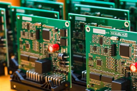
Effective PCB assembly and manufacturing demand a strategic combination of design foresight, material selection, and process optimization. Central to this is precision soldering, which ensures reliable electrical connections in PCBA (Printed Circuit Board Assembly). Modern workflows integrate automated quality control systems, such as automated optical inspection (AOI), to detect micro-scale defects in real time.
| Factor | Traditional Approach | Advanced Strategy |
|---|---|---|
| Soldering Accuracy | Manual inspection | Laser-assisted soldering |
| Defect Detection | Sampling-based checks | In-line AOI systems |
| Thermal Management | Passive heat sinks | Embedded thermal vias |
For mission-critical applications, selecting high-frequency substrates like Rogers 4350B minimizes signal loss, while stacked microvias enhance connectivity in high-density layouts. Streamlining PCB assembly workflows requires balancing automation with human expertise—particularly in prototyping phases where flexibility is key. Future-proofing involves adopting IoT-enabled monitoring to predict equipment wear, ensuring uninterrupted PCBA production cycles. By aligning material innovation with process rigor, manufacturers achieve repeatable quality across complex electronics.
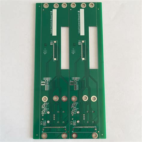
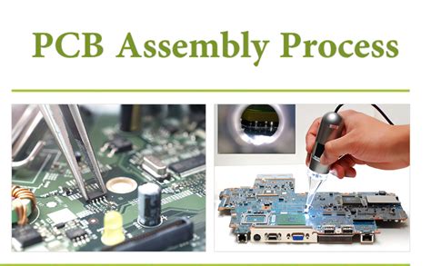
Precision Soldering in PCB Assembly
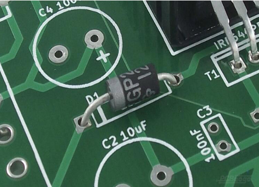
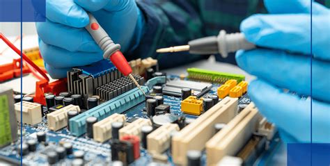
Achieving reliable connections in PCB assembly hinges on precision soldering techniques that balance speed with microscopic accuracy. Modern PCBA processes leverage advanced methods like reflow soldering with nitrogen atmospheres, which reduce oxidation while maintaining consistent thermal profiles across densely populated boards. Selective soldering systems further enhance this precision, targeting specific components without affecting heat-sensitive parts—a critical capability for mixed-technology boards containing both through-hole and surface-mount devices.
The choice of solder paste composition directly impacts joint integrity, with lead-free SAC305 alloys now dominating mission-critical applications due to their superior thermal fatigue resistance. Automated dispensing systems ensure micron-level accuracy in paste deposition, particularly for ultra-fine-pitch components below 0.4mm spacing. Concurrently, real-time thermal imaging monitors heat distribution during soldering, preventing cold joints or component damage caused by thermal stress gradients.
For high-reliability PCB assembly, surface finish selection—whether ENIG, immersion silver, or HASL—interacts synergistically with soldering parameters to optimize wettability and intermetallic bonding. Emerging laser-assisted soldering technologies address challenges in miniaturized assemblies, enabling sub-100µm connections with repeatable void rates under 5%. Post-soldering validation combines automated optical inspection (AOI) with X-ray tomography to verify hidden connections, completing a quality chain where precision soldering serves as the foundational link for durable electronic systems.
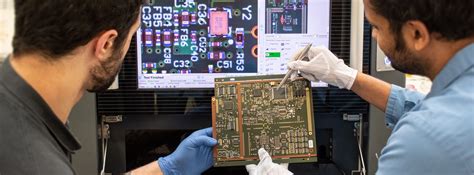
Automated Quality Control for PCBs
Modern PCB assembly processes demand rigorous inspection protocols to meet mission-critical reliability standards. Automated systems now integrate machine vision, AI-powered defect recognition, and 3D X-ray scanning to detect microscopic flaws in PCBA components – from solder bridging to misplaced resistors – with submicron accuracy. These systems analyze up to 10,000 inspection points per minute, achieving defect detection rates exceeding 99.95% compared to manual methods.
Advanced statistical process control algorithms cross-reference real-time data from automated optical inspection (AOI) systems with historical production metrics, enabling predictive maintenance of pick-and-place machines and reflow ovens. For high-density boards, multi-spectral imaging identifies thermal stress patterns invisible to conventional cameras, while in-circuit test (ICT) fixtures validate electrical continuity across complex circuit paths.
The shift toward Industry 4.0-compliant PCBA workflows allows manufacturers to correlate quality metrics with specific production batches, creating闭环 feedback for continuous process optimization. This data-driven approach reduces false rejection rates by 40% while maintaining compliance with IPC-A-610 and J-STD-001 standards – a critical advantage for aerospace and medical electronics applications where zero-defect tolerance governs manufacturing protocols.
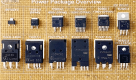
Advanced Materials for Robust Circuit Boards
The reliability of PCB assembly processes hinges on material science innovations that address thermal, mechanical, and electrical stresses. Modern high-performance substrates, such as polyimide flex materials and ceramic-filled laminates, provide exceptional thermal stability, with glass transition temperatures (Tg) exceeding 180°C. These materials minimize warping during PCBA reflow cycles while maintaining signal integrity in high-frequency applications.
"Selecting substrate materials with matched coefficients of thermal expansion (CTE) is critical for preventing delamination in multilayer boards exposed to extreme temperature fluctuations."
For mission-critical applications, halogen-free prepregs and low-loss dielectrics reduce signal attenuation in high-speed circuits, while advanced conformal coatings like parylene enhance moisture resistance. Innovations in conductive adhesives and solder alloys—such as SAC305 variants with nickel additives—improve joint durability under vibration-prone environments.
When designing for harsh operating conditions, engineers should prioritize materials with verified IPC-4101 certifications and compatibility with automated PCB assembly workflows. Recent advancements in nanoparticle-reinforced resins further extend board lifespan by mitigating electromigration risks in high-current traces.
Transitioning to these advanced materials requires collaboration between design teams and PCBA manufacturers to balance performance gains with manufacturability constraints, ensuring seamless integration into next-generation electronics.
Mission-Critical PCB Design Best Practices
When developing printed circuit boards for aerospace, medical, or industrial automation systems, PCB assembly reliability becomes non-negotiable. Designers must prioritize signal integrity by implementing controlled impedance routing and minimizing crosstalk through strategic layer stacking. For PCBA destined for harsh environments, material selection shifts toward high-Tg laminates and conformal coatings that withstand thermal cycling and chemical exposure.
A proactive approach to redundancy involves integrating backup traces for critical power delivery networks and using via-in-pad structures to enhance mechanical stability. Advanced simulation tools, such as electromagnetic field analyzers, help validate high-speed signal paths before prototyping—a crucial step when lead times for mission-critical PCB assembly exceed standard production schedules.
Thermal management strategies should align with the final application’s operational profile. For instance, embedding copper-filled vias beneath high-power components reduces junction temperatures by 15–20% in compact PCBA layouts. Collaboration between design engineers and contract manufacturers during design-for-manufacturability (DFM) reviews ensures compliance with IPC-6012 Class 3 standards, which govern reliability requirements for life-support systems and military hardware.
Implementing these practices requires balancing performance metrics with cost constraints—a challenge mitigated through iterative prototyping and automated testing protocols. By anchoring decisions in application-specific failure mode analyses, teams can optimize both functionality and longevity in mission-critical electronics.
Streamlining PCB Assembly Workflows
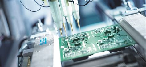
Efficient PCB assembly processes are critical for meeting the demands of modern electronics production. By implementing design for manufacturing (DFM) principles early in the design phase, engineers can minimize rework and reduce material waste. Automated pick-and-place systems, combined with optimized solder paste application, accelerate PCBA throughput while maintaining consistency across high-volume batches.
Lean manufacturing methodologies, such as just-in-time inventory management and standardized work instructions, further refine workflow efficiency. For instance, integrating enterprise resource planning (ERP) software with PCB assembly lines enables real-time tracking of component availability, preventing bottlenecks caused by missing parts. Advanced manufacturers are also adopting modular production layouts, allowing rapid reconfiguration for different product lines without sacrificing precision.
Transitioning to paperless workflows through digital work orders and machine-to-machine communication reduces human error and accelerates traceability. This approach aligns with the broader focus on automated quality control discussed in later sections, ensuring seamless data flow from assembly to inspection stages. By prioritizing workflow optimization, companies can achieve shorter lead times, lower costs, and improved scalability in PCBA production—key factors for staying competitive in mission-critical electronics markets.
Automated Optical Inspection Techniques
Modern pcb assembly lines leverage Automated Optical Inspection (AOI) systems to achieve micron-level accuracy in defect detection. These systems employ high-resolution cameras and machine vision algorithms to scan pcba units, verifying solder joint quality, component alignment, and trace integrity. Unlike manual inspections, AOI operates at speeds exceeding 10,000 components per hour while maintaining sub-0.1mm precision, making it indispensable for high-volume production of mission-critical electronics.
Advanced AOI platforms integrate deep learning models to differentiate between acceptable process variations and critical flaws like solder bridges or tombstoned capacitors. By cross-referencing design files with real-time imaging data, these systems flag deviations as small as 25μm, enabling immediate corrections in the pcb assembly workflow. Recent innovations include 3D AOI, which adds Z-axis profiling to detect coplanarity issues in Ball Grid Array (BGA) components—a common failure point in aerospace and medical pcba applications.
The technology’s statistical process control capabilities also feed data back to solder paste printers and pick-and-place machines, creating a closed-loop quality ecosystem. This proactive approach reduces rework rates by up to 65% compared to traditional end-of-line testing, aligning with industry demands for zero-defect manufacturing in complex multilayer boards.
Thermal Management in High-Density PCBs
Effective thermal management is critical in modern high-density PCB assembly, where component miniaturization and increased power demands create unprecedented heat challenges. Engineers leverage advanced thermal vias and embedded cooling channels to dissipate heat efficiently in compact designs. For PCBA applications requiring extreme reliability, such as aerospace or medical devices, materials like metal-core substrates or ceramic-filled laminates provide superior thermal conductivity while maintaining electrical integrity.
Automated PCB assembly processes now integrate infrared thermal imaging during quality checks, enabling real-time detection of hotspots before final testing. Strategic component placement algorithms optimize airflow in multilayer boards, reducing thermal stress on sensitive components. Innovations like phase-change materials and active cooling systems are increasingly adopted in mission-critical PCBA projects to maintain operational stability under fluctuating thermal loads.
Designers must balance thermal performance with signal integrity, often employing thermal simulation software to predict heat distribution across complex layouts. Compliance with IPC-2221B standards ensures proper clearance for heat dissipation in high-current traces. As PCB assembly scales for IoT and 5G applications, robust thermal strategies directly impact product lifespan, making this a cornerstone of next-generation electronics manufacturing.
Future-Proofing PCB Manufacturing Pr
To ensure long-term viability in PCB assembly and manufacturing, engineers must adopt adaptable strategies that account for evolving technological demands. A critical approach involves integrating modular design principles into PCBA workflows, enabling rapid component upgrades without complete board redesigns. This flexibility becomes essential as IoT devices and 5G infrastructure push the boundaries of circuit density and signal integrity requirements.
Leading manufacturers now implement digital twin simulations to stress-test designs under hypothetical future operating conditions, from extreme thermal cycling to electromagnetic interference scenarios. Pairing this with AI-driven predictive maintenance in production lines reduces downtime while extending equipment lifespan—a key factor in maintaining cost efficiency.
Material innovation plays an equally vital role in future readiness. The adoption of high-Tg laminates and halogen-free substrates addresses both environmental regulations and performance demands for high-frequency applications. When combined with automated optical inspection systems capable of learning new defect patterns, these advancements create manufacturing ecosystems that scale with emerging Industry 4.0 standards.
By balancing forward-looking R&D investments with backward-compatible PCB assembly processes, companies can navigate market shifts while maintaining backward compatibility for legacy systems—a dual capability that separates industry leaders from competitors.
Conclu
The evolution of PCB assembly and PCBA processes underscores the necessity of integrating precision engineering with scalable manufacturing frameworks. As industries demand higher reliability for mission-critical applications, manufacturers must adopt a holistic approach that balances advanced materials with automated inspection protocols. Key innovations in thermal management solutions and automated optical inspection (AOI) systems have set new benchmarks for defect detection and long-term board durability.
Looking ahead, the emphasis on future-proofing production lines will drive investments in modular PCBA workflows and AI-driven analytics. These strategies not only mitigate risks in high-density designs but also enhance adaptability to emerging technologies like IoT and 5G. By prioritizing cross-functional collaboration between design and manufacturing teams, stakeholders can accelerate time-to-market while maintaining stringent quality standards.
Ultimately, the success of PCB assembly hinges on continuous improvement cycles that leverage data from real-time process monitoring and predictive maintenance tools. This proactive stance ensures robust circuit boards capable of meeting both current performance thresholds and tomorrow’s technical challenges.
FAQ
What design factors most impact reliability in pcb assembly?
Component placement accuracy, solder joint integrity, and material compatibility directly affect PCBA reliability. Designs must account for thermal expansion coefficients and signal integrity requirements, especially in high-density layouts.
How does automated inspection improve pcb manufacturing quality?
Automated Optical Inspection (AOI) systems detect micro-scale defects like solder bridges or missing components with 99.9% accuracy, reducing human error. This aligns with Industry 4.0 standards for traceability in mission-critical applications.
Are specialized materials necessary for high-temperature pcb assembly environments?
Yes. High-Tg FR-4, polyimide substrates, and ceramic-filled laminates withstand thermal stress better than standard materials. These are essential for aerospace or automotive PCBA applications where operating temperatures exceed 150°C.
What certifications ensure quality in pcb manufacturing?
IPC-A-610 (acceptability) and IPC-J-STD-001 (soldering) certifications validate adherence to industry benchmarks. ISO 9001 and IATF 16949 further guarantee process consistency for automotive-grade PCBA production.
How can manufacturers future-proof pcb assembly workflows?
Implementing modular design principles and investing in solder paste jetting systems allow rapid adaptation to new component packages. Real-time process monitoring via IoT-enabled PCBA lines also enhances scalability.
Optimize Your Next Project with Expert PCB Assembly
For tailored solutions integrating these advanced strategies, please click here to consult our PCBA engineering team.