Advanced Techniques for Optimizing PCBA Circuit Board Performance

Key Takeaways
Effective optimization of PCBA circuit boards requires a multifaceted approach integrating thermal management, signal integrity protocols, and precision PCB assembly techniques. Key strategies include implementing advanced thermal interface materials to mitigate heat buildup, which directly impacts long-term reliability in high-density designs. Engineers must prioritize impedance matching and crosstalk reduction during layout planning to maintain signal integrity across high-speed traces.
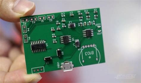
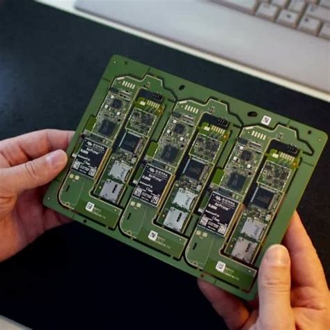
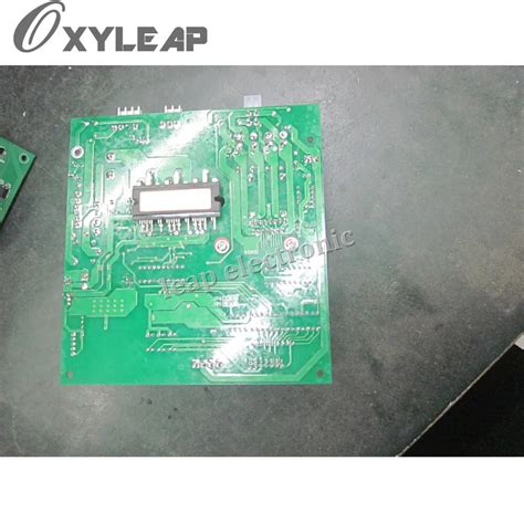
Modern PCBA manufacturing benefits from laser-direct imaging and automated optical inspection systems, ensuring micron-level accuracy in component placement. Material selection plays a pivotal role, with high-Tg substrates and low-loss dielectrics enhancing performance in demanding environments. Rigorous in-circuit testing combined with boundary-scan diagnostics validates PCBA functionality before deployment, reducing field failure risks.
Emerging trends like embedded passives and 3D-printed circuitry are reshaping PCB assembly paradigms, while intelligent layer stackup configurations optimize electromagnetic compatibility. These advancements collectively address EMI challenges and power distribution inefficiencies, establishing a foundation for next-generation PCBA circuit boards capable of supporting 5G and IoT applications.
Thermal Management Solutions for PCBA Reliability
Effective thermal management is critical for ensuring the long-term reliability of PCBA (Printed Circuit Board Assembly) systems, particularly in high-power or densely packed electronic devices. As component miniaturization accelerates, managing heat dissipation becomes a central challenge in PCB assembly design. Engineers employ thermal vias and copper pours to distribute heat evenly across the board, preventing localized hotspots that degrade solder joints or semiconductor performance. Advanced solutions like embedded heat sinks or thermally conductive adhesives further enhance heat transfer from critical components such as power ICs or processors.
Material selection plays a pivotal role: substrates with high glass transition temperatures (Tg) and low coefficients of thermal expansion (CTE) minimize warping under thermal stress. For applications requiring extreme thermal stability, ceramic-filled laminates or metal-core PCBA designs offer superior performance. Computational fluid dynamics (CFD) simulations are increasingly used to model airflow and optimize heatsink placement during the PCB assembly phase. Additionally, conformal coatings with thermal dissipation properties protect sensitive circuits while aiding in heat redistribution.
By integrating these strategies, manufacturers achieve a balance between thermal efficiency and mechanical integrity, ensuring PCBA reliability across varying operational conditions—from consumer electronics to industrial automation systems. This proactive approach to thermal management directly supports the broader goals of signal integrity and EMI reduction outlined in subsequent sections.
Signal Integrity Optimization in PCBA Circuit Design
Achieving optimal signal integrity in PCBA design requires a systematic approach to minimize noise, distortion, and timing errors. Critical factors include impedance control, trace routing strategies, and via optimization. For high-speed circuits, mismatched impedances between components can lead to signal reflections, degrading performance. Implementing controlled impedance routing and minimizing trace lengths between critical nodes, such as clock generators or high-frequency ICs, ensures cleaner signal propagation.
Tip: Use differential pair routing for high-speed signals like USB or HDMI to reduce electromagnetic interference (EMI) and crosstalk.
| Technique | Key Parameters | Impact on Signal Integrity |
|---|---|---|
| Impedance Matching | Trace width, spacing | Reduces reflections |
| Crosstalk Mitigation | Guard traces, spacing | Lowers noise coupling |
| Via Optimization | Stub length, pad size | Minimizes signal path discontinuities |
In PCB assembly, material selection plays a pivotal role. Substrates with stable dielectric constants (e.g., FR-4 with low-loss variants) help maintain consistent impedance across temperature fluctuations. Additionally, avoiding sharp angles in trace routing and optimizing layer stackups to separate analog and digital grounds are essential for minimizing interference.
Advanced simulation tools, such as SPICE or SI/PI analyzers, enable designers to model signal behavior pre-production, identifying bottlenecks like resonance or attenuation. For multi-layer PCBA designs, proper decoupling capacitor placement near power pins suppresses voltage fluctuations, further stabilizing signal paths. By integrating these strategies, engineers can ensure robust performance in high-frequency and high-density applications.
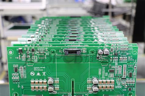
Precision Manufacturing Techniques for Enhanced PCBA Performance
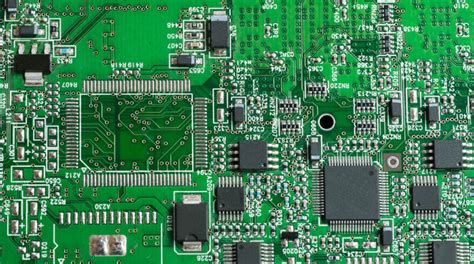
Modern PCBA production demands micron-level accuracy to meet the performance requirements of advanced electronics. Central to this process is PCB assembly technology that integrates automated optical inspection (AOI) systems, which detect solder joint defects as small as 10μm, ensuring 99.98% component placement accuracy. High-precision pick-and-place machines, calibrated for 0.025mm tolerances, enable consistent mounting of miniature components like 0201 resistors or 0.4mm-pitch BGAs.
To minimize thermal stress during reflow, manufacturers employ closed-loop temperature profiling, dynamically adjusting heating zones to match solder paste specifications. This prevents warping or delamination in multi-layer PCBA designs. Laser-direct imaging (LDI) further refines circuit patterning, achieving trace widths below 25μm for high-density interconnects while reducing etching errors by 40% compared to traditional photolithography.
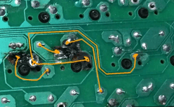
Advanced stencil printing techniques, utilizing nano-coated squeegees and step-down apertures, ensure uniform solder paste deposition across mixed-component boards. Combined with in-line 3D SPI (solder paste inspection), this reduces rework rates by 60% in PCB assembly workflows. Such precision extends to conformal coating applications, where robotic dispensers apply 10–50μm protective layers with ±5% thickness variation, safeguarding PCBA units against environmental stressors without compromising signal integrity.
These methodologies not only elevate production quality but directly align with preceding thermal and signal integrity strategies, forming a cohesive framework for optimizing PCBA reliability across operational lifetimes.
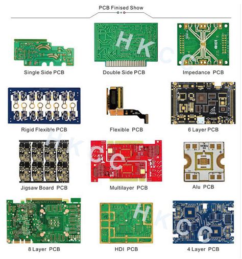
Material Selection Strategies for High-Efficiency PCBA Boards
Effective PCBA performance begins with strategic material selection, a critical factor influencing thermal stability, electrical conductivity, and long-term reliability. The choice of substrate material forms the foundation, with high-Tg (glass transition temperature) laminates like FR-4 or polyimide offering enhanced resistance to thermal stress during PCB assembly and operation. For high-frequency applications, low-loss dielectric materials such as Rogers RO4000® series minimize signal attenuation, directly supporting signal integrity optimization.
Conductive materials also demand precision: copper thickness and purity impact current-carrying capacity, while advanced surface finishes like ENIG (Electroless Nickel Immersion Gold) ensure robust solderability and corrosion resistance. In thermally demanding environments, incorporating metal-core substrates or ceramic-filled prepregs improves heat dissipation, aligning with broader thermal management solutions.
Adhesives and solder masks must balance mechanical durability with electrical insulation. Halogen-free solder masks meet environmental standards without compromising performance, while thermally conductive adhesives enhance component bonding in compact PCBA designs. By aligning material properties with operational requirements—whether for automotive, aerospace, or IoT applications—engineers can optimize both manufacturing yield and end-product efficiency. This systematic approach ensures that every layer of the circuit board contributes to peak performance across its lifecycle.
Advanced Testing Methods for PCBA Performance Validation
Validating PCBA performance requires a systematic approach that combines cutting-edge tools with rigorous analysis protocols. Modern manufacturers employ automated optical inspection (AOI) to detect PCB assembly defects like solder bridging or component misalignment, achieving accuracy rates exceeding 99.5%. For hidden flaws, X-ray inspection penetrates multilayer boards to identify voids in ball grid arrays (BGAs) or microcracks in interconnects.
Electrical validation relies on in-circuit testing (ICT) to verify signal integrity and power distribution across the PCBA, ensuring compliance with design specifications. High-frequency boards demand vector network analysis (VNA) to measure impedance mismatches and insertion losses, critical for maintaining signal fidelity in 5G or IoT applications.
Environmental stress testing simulates real-world conditions through thermal cycling (-40°C to +125°C) and humidity exposure, assessing PCBA reliability under extreme operational demands. Advanced labs integrate boundary scan testing for complex boards with embedded processors, enabling firmware-level diagnostics without physical probe access.
To address emerging challenges, machine vision-assisted functional testing validates end-to-end performance by replicating user interactions with millimeter precision. These methods collectively reduce field failure rates by up to 70% while aligning with ISO 9001 and IPC-A-610 standards. By combining automated and scenario-based assessments, engineers ensure PCB assembly outcomes meet both functional benchmarks and long-term durability requirements.
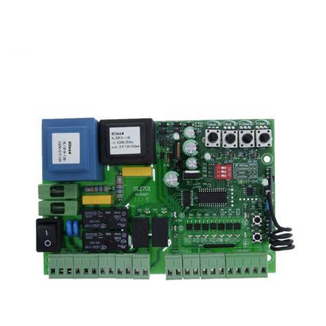
PCBA Circuit Board Design Best Practices for EMI Reduction
Effective EMI reduction in PCBA circuit board design begins with strategic layout planning and material integration. A critical step involves implementing ground planes to create low-impedance return paths, which minimizes electromagnetic radiation from high-speed traces. For PCB assembly processes, maintaining proper spacing between analog and digital components reduces inductive coupling, while partitioning noise-sensitive circuits into isolated zones prevents interference propagation.
Incorporating shielding techniques such as conductive coatings or metal enclosures around high-frequency components further suppresses unwanted emissions. Designers should prioritize PCBA designs with optimized trace routing—using 45-degree angles instead of 90-degree bends lowers harmonic generation by up to 20%. Additionally, employing differential signaling for critical interfaces enhances noise immunity without compromising signal integrity.
Layer stackup configuration plays a pivotal role: placing power and ground layers adjacent to signal layers creates natural Faraday cages. Simulations using electromagnetic field solvers during the design phase help identify hotspots, enabling preemptive adjustments. For pcb assembly workflows, selecting low-loss dielectric materials (e.g., Rogers 4350B) reduces parasitic capacitance, which is particularly vital for RF-focused boards.
Combining these practices with rigorous post-production testing—such as near-field scans—ensures compliance with international EMI standards while preserving the PCBA circuit board’s functional efficiency.
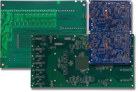
Maximizing PCBA Efficiency Through Layer Stackup Innovations
Effective PCBA performance begins with intelligent layer stackup design, a critical factor in balancing signal integrity, thermal dissipation, and electromagnetic compatibility. By optimizing the arrangement of conductive and dielectric layers, engineers can minimize PCB assembly complexities while enhancing electrical performance. For high-speed applications, impedance-controlled routing becomes achievable through precise dielectric material selection and layer thickness calibration, reducing signal loss and crosstalk.
Strategic placement of power and ground planes within the stackup not only stabilizes voltage distribution but also acts as a shield against electromagnetic interference (EMI). For instance, embedding ground layers adjacent to high-frequency signal traces mitigates noise propagation, aligning with broader EMI reduction strategies. Additionally, thermal vias integrated into the stackup improve heat dissipation, complementing thermal management solutions discussed earlier.
Modern PCBA designs increasingly adopt asymmetric stackups to accommodate mixed-signal environments, where analog and digital circuits coexist. This approach allows isolation of sensitive components while maintaining compact form factors. Advanced simulation tools further validate layer configurations, ensuring manufacturability and reliability during PCB assembly. As layer count grows, material choices—such as low-loss laminates or high-Tg substrates—play a pivotal role in sustaining performance under demanding operational conditions.
By harmonizing layer stackup innovations with precision manufacturing, engineers unlock new thresholds of PCBA efficiency, setting the stage for next-generation electronic systems.
Future Trends in PCBA Circuit Board Optimization Technologies
The evolution of PCBA optimization is increasingly driven by emerging technologies that address the growing demand for miniaturization, energy efficiency, and high-speed functionality. Artificial intelligence (AI) and machine learning (ML) are revolutionizing PCB assembly processes by enabling predictive analytics for defect detection and automated design adjustments. These systems analyze vast datasets from past production runs to refine component placement, reduce parasitic capacitance, and optimize thermal pathways in real time. Another critical trend involves the integration of advanced materials, such as ultra-low-loss laminates and embedded passive components, which enhance signal integrity while reducing board footprint.
Industry leaders are also prioritizing sustainable manufacturing practices, including lead-free solder alloys and recyclable substrates, to align with global environmental regulations. Additionally, the adoption of 3D-printed electronics is gaining traction, allowing for rapid prototyping of complex PCBA layouts with embedded sensors or antennas. Innovations in heterogeneous integration—combining silicon, GaN, and organic substrates—are pushing the boundaries of power density and thermal management. As IoT and 5G networks expand, PCB assembly techniques will increasingly focus on modular designs that support seamless firmware updates and real-time performance monitoring. These advancements ensure PCBA technology remains at the forefront of next-generation electronic systems.
Conclusion
In modern electronics, optimizing PCBA performance demands a multifaceted approach that integrates cutting-edge design principles with precision manufacturing. By implementing advanced thermal management strategies and maintaining rigorous signal integrity protocols, engineers can significantly enhance the reliability of PCB assembly processes. The convergence of high-precision fabrication techniques and intelligent material selection creates boards capable of meeting increasingly demanding operational requirements.
Emerging technologies like AI-driven analytics and IoT-enabled monitoring systems are redefining performance validation methods, enabling real-time adjustments during production. As industries push toward miniaturization and higher power densities, adopting adaptive layer stackup configurations becomes critical for minimizing electromagnetic interference and ensuring signal clarity.
Successful PCBA optimization ultimately hinges on balancing innovative engineering solutions with robust quality control measures. By staying attuned to evolving industry standards and leveraging data-driven insights, manufacturers can achieve sustained improvements in both efficiency and durability across electronic systems.
FAQs
What are the primary factors affecting thermal performance in PCBA designs?
Effective thermal management in PCBA circuit boards relies on proper component placement, copper pour techniques, and the use of thermally conductive substrates. Implementing heat sinks or thermal vias can further dissipate excess energy, ensuring long-term reliability.
How does signal integrity optimization impact PCBA functionality?
Maintaining signal integrity minimizes data loss and electromagnetic interference (EMI). Techniques like impedance matching, controlled trace routing, and ground plane optimization are critical for high-speed PCB assembly applications, particularly in RF and digital systems.
What role does material selection play in high-efficiency PCBA boards?
Choosing materials with low dielectric loss and high thermal stability, such as FR-4 HTG or polyimide substrates, enhances PCBA performance. Advanced laminates also improve signal propagation speeds while reducing crosstalk in dense layouts.
Why are advanced testing methods essential for PCBA validation?
Automated optical inspection (AOI) and in-circuit testing (ICT) identify manufacturing defects like solder bridges or open circuits. Environmental stress screening (ESS) ensures boards withstand operational extremes, aligning with precision manufacturing standards.
How can layer stackup design improve PCBA efficiency?
Optimizing layer stackups reduces EMI and improves power distribution. Strategic placement of ground planes and signal layers in PCBA circuit boards minimizes parasitic capacitance, enhancing signal clarity and reducing noise.
Ready to Optimize Your PCBA Circuit Board Performance?
For expert PCB assembly services and tailored solutions, please click here to explore advanced manufacturing capabilities that meet your project’s technical demands.