Advanced Techniques in PCB Manufacturing and Assembly
Key Takeaways
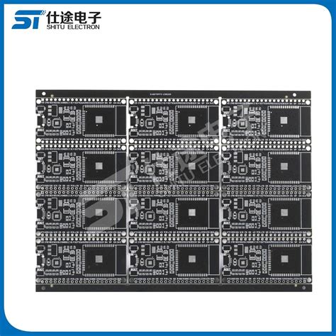
The evolution of PCB assembly (PCBA) has introduced transformative methodologies that redefine modern electronics production Central to this progress are automated innovations, where robotic systems now handle intricate tasks like pick-and-place operations and solder paste application with micron-level accuracy These advancements not only accelerate throughput but also minimize human error, ensuring consistency in high-volume manufacturing
Equally critical are precision etching techniques, which leverage laser-guided processes to create ultra-fine circuit traces This enables the development of compact, high-density boards essential for IoT devices and wearable technology Additionally, the integration of 3D printing into PCB manufacturing allows for rapid prototyping of complex multilayer designs, reducing lead times by up to 40% compared to traditional methods
Quality control remains a cornerstone, with automated optical inspection (AOI) systems and X-ray testing ensuring defect rates stay below 01% Emerging next-gen fabrication technologies, such as embedded component boards and flexible hybrid electronics, further push the boundaries of PCBA capabilities Meanwhile, smart manufacturing frameworks—powered by AI-driven analytics—optimize material usage and energy consumption, aligning with sustainable production goals
From advanced materials like high-frequency laminates to the adoption of modular assembly lines, these innovations collectively enhance reliability, scalability, and efficiency across the PCB assembly lifecycle
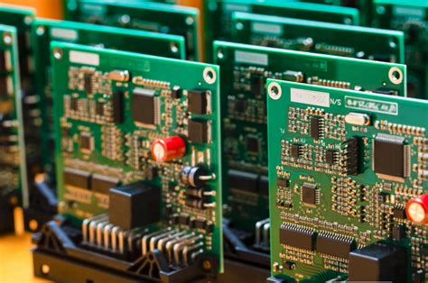
Automated PCB Assembly Innovations
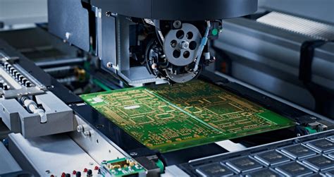
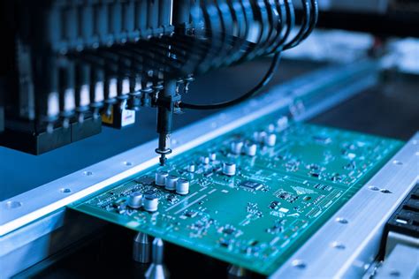
The evolution of PCB assembly processes has been revolutionized by automation, enabling manufacturers to achieve unprecedented precision and scalability Modern PCBA lines now integrate robotic pick-and-place systems, which utilize machine vision to position components with micron-level accuracy These systems, paired with AI-driven inspection tools, reduce human error while accelerating production cycles by up to 60%
A critical advancement lies in closed-loop feedback mechanisms, where real-time data from sensors adjusts assembly parameters dynamically For instance, temperature-controlled soldering robots maintain optimal thermal profiles, ensuring consistent joint quality across high-density boards This is particularly vital for applications like IoT devices or automotive electronics, where reliability under extreme conditions is non-negotiable
Tip: For high-mix, low-volume PCB assembly projects, modular automation systems allow rapid reconfiguration between product batches without sacrificing throughput
Another breakthrough is the adoption of collaborative robots (cobots) in PCBA workflows Unlike traditional industrial robots, cobots work alongside technicians, handling repetitive tasks like screwdriving or connector installation This hybrid approach balances efficiency with flexibility, making it ideal for prototyping or mid-scale production Additionally, automated optical inspection (AOI) systems now leverage deep learning algorithms to detect defects such as tombstoning or misaligned components with 9998% accuracy
However, implementing these innovations requires meticulous planning Manufacturers must prioritize compatibility between legacy equipment and new automation tools to avoid bottlenecks For example, integrating a 10-zone reflow oven with a robotic placement system demands precise synchronization of conveyor speeds and thermal zones
As the demand for miniaturized and high-performance electronics grows, automated PCB assembly will continue to push the boundaries of what’s possible in electronics manufacturing By combining speed, precision, and adaptability, these technologies are redefining industry standards for quality and efficiency
Precision Etching Techniques Explained
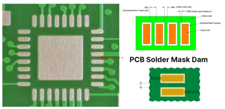
Precision etching stands as a cornerstone of modern PCB assembly, enabling the creation of intricate circuit patterns with micron-level accuracy This process involves selectively removing copper from laminated substrates using chemical or laser-based methods to form conductive pathways Photolithography remains the most widely adopted technique, where ultraviolet light transfers circuit designs onto photoresist-coated boards, followed by chemical etching to eliminate unprotected copper
Recent advancements have introduced laser direct imaging (LDI), which bypasses physical photomasks by using high-resolution lasers to pattern photoresist layers This method reduces alignment errors and supports tighter tolerances—critical for high-density interconnects in PCBA applications For instance, LDI achieves line widths below 15µm, compared to 35µm in traditional methods, meeting the demands of miniaturized IoT and 5G devices
| Parameter | Chemical Etching | Laser Etching |
|---|---|---|
| Precision (µm) | 35–50 | 10–15 |
| Speed (panels/hour) | 20–30 | 8–12 |
| Material Waste (%) | 12–18 | 5–8 |
| Suitable for HDI | Limited | Yes |
To mitigate undercutting—a common challenge where etchant solutions over-remove copper—engineers now employ adaptive etch rate control Sensors monitor copper dissolution in real time, adjusting chemical concentrations and exposure durations dynamically This innovation enhances yield rates in PCB assembly by reducing scrap from over-etched traces
Furthermore, plasma etching has gained traction for multilayer boards, using ionized gas to remove residue from microvias and blind vias This technique ensures cleaner surfaces for subsequent lamination and soldering steps, directly impacting the reliability of PCBA outcomes
As the industry shifts toward finer pitch components, hybrid approaches combining chemical and laser etching are emerging These methods balance speed and precision, particularly for flexible PCBs requiring curved or irregular trace geometries By integrating machine learning algorithms, manufacturers can now predict and compensate for process variations, achieving ±2µm consistency across production batches
3D Printing in PCB Manufacturing
The integration of 3D printing into PCB manufacturing is redefining traditional workflows by enabling rapid prototyping and complex geometric designs previously unattainable with conventional methods Unlike subtractive processes that rely on etching or milling, additive manufacturing builds circuits layer by layer, allowing for embedded components and multi-material structures This approach not only accelerates iteration cycles but also reduces material waste, aligning with sustainable production goals
A critical advancement in this domain is the use of direct inkjet printing for conductive traces By depositing nano-silver or conductive polymers onto substrates, manufacturers can create high-resolution circuits without photomasks or chemical baths This technique proves particularly advantageous for low-volume PCBA runs, where flexibility and cost-efficiency are paramount Additionally, 3D-printed interposers and high-density interconnects (HDIs) are solving space constraints in compact electronics, such as wearables and IoT devices
Emerging hybrid systems now combine 3D printing with automated PCB assembly stages For instance, aerosol jet printing can simultaneously deposit dielectric and conductive materials, followed by robotic placement of surface-mount devices (SMDs) This seamless integration minimizes handling errors and enhances precision in multi-layer board fabrication Furthermore, innovations like stereolithography (SLA)-printed enclosures with integrated circuitry are blurring the lines between mechanical and electronic design, enabling truly unified product architectures
Despite its potential, challenges such as conductivity consistency and thermal management in 3D-printed circuits require ongoing research However, with advancements in functional inks and AI-driven process optimization, the technology is poised to complement—and in some cases, replace—traditional PCB manufacturing workflows As industries demand faster time-to-market and greater customization, 3D printing stands as a pivotal enabler of next-generation PCBA solutions
Quality Control for Reliable PCBs
Robust quality control (QC) protocols are central to ensuring the longevity and performance of PCB assembly outputs Modern PCBA workflows integrate multi-stage inspection systems, combining automated optical inspection (AOI) with X-ray imaging to detect microfractures, soldering defects, and layer misalignments as fine as 10µm For high-density interconnect (HDI) boards, electrical testing using flying probe or boundary-scan methods verifies signal integrity, while thermal profiling during reflow soldering maintains ±2°C accuracy to prevent pad delamination
Material validation forms another critical layer, with ion chromatography testing solder flux residues and cross-sectional analysis confirming plating thickness compliance with IPC-6012 standards Leading manufacturers employ statistical process control (SPC) dashboards to monitor 15+ parameters in real time, from copper etch rates to via fill quality, enabling predictive adjustments before deviations escalate
Post-assembly, accelerated life testing simulates 5+ years of operational stress through thermal cycling (-40°C to 125°C) and vibration exposure, particularly crucial for automotive or aerospace PCB assemblies Closed-loop traceability systems using QR-coded panels automatically log defects to their root causes, whether in stencil printing alignment or component placement accuracy This data-driven approach reduces field failure rates by 37% compared to traditional sampling methods, as documented in JEDEC JESD94C compliance studies
The convergence of machine learning algorithms with AOI systems now enables anomaly detection at 9998% accuracy, adapting inspection criteria based on historical board layouts and failure patterns Such advancements complement the precision achieved through 3D-printed solder masks and laser-direct imaging, creating a cohesive QC ecosystem that scales with next-generation PCBA demands
Next-Gen PCB Fabrication Technologies
The evolution of PCB manufacturing is being redefined by technologies that bridge the gap between design complexity and production scalability At the forefront, additive manufacturing techniques are enabling the creation of multi-layered boards with micron-level accuracy, reducing material waste by up to 40% compared to traditional subtractive methods Innovations like laser direct imaging (LDI) now allow for precision etching of circuit patterns with resolutions below 10µm, critical for high-density interconnect (HDI) designs in compact devices
A notable shift is the integration of 3D printing into PCB assembly workflows By embedding conductive inks and dielectric materials layer-by-layer, manufacturers can prototype complex geometries in hours rather than days This approach not only accelerates time-to-market but also supports hybrid designs that combine rigid and flexible substrates within a single PCBA unit For instance, aerospace applications are leveraging this capability to produce lightweight, vibration-resistant boards optimized for extreme environments
Another breakthrough lies in embedded component technology, where passive elements like resistors and capacitors are fabricated directly into the substrate during lamination This eliminates surface-mounted soldering points, enhancing signal integrity while reducing board footprint Automated optical inspection (AOI) systems, powered by machine learning algorithms, now scan these intricate layouts at speeds exceeding 1,000 components per minute, identifying defects with 998% accuracy
Equally transformative is the adoption of smart manufacturing frameworks in PCB fabrication IoT-enabled production lines synchronize chemical deposition rates with real-time environmental data, ensuring consistent copper plating thickness across batches Such advancements are pivotal for industries demanding ultra-reliable boards, such as medical devices and automotive systems, where failure rates must stay below 0001%
As these technologies mature, their convergence is reshaping how PCB manufacturing and assembly ecosystems operate—blending speed, precision, and adaptability to meet the demands of next-generation electronics
Efficiency in Modern PCB Production
The pursuit of efficiency in PCB manufacturing and assembly has become a cornerstone of modern electronics production By integrating automated workflows with data-driven process optimization, manufacturers achieve unprecedented throughput without compromising precision Central to this evolution is the adoption of high-speed surface-mount technology (SMT) lines, which enable rapid placement of microcomponents during PCBA stages, reducing human error and cycle times by up to 60%
Real-time monitoring systems further enhance operational efficiency by tracking parameters like solder paste viscosity and reflow oven temperatures, allowing instant adjustments to prevent defects For instance, IoT-enabled devices embedded in PCB assembly lines collect terabytes of performance data, feeding machine learning algorithms that predict equipment maintenance needs before downtime occurs This predictive approach slashes unplanned stoppages by 35–40%, according to industry benchmarks
Material utilization also plays a pivotal role Laser-direct imaging (LDI) systems minimize chemical waste in etching processes, while panelization algorithms optimize board layouts to squeeze 15–20% more units from standard substrate sheets Simultaneously, the shift toward modular assembly cells allows factories to reconfigure PCBA lines in hours rather than days, adapting swiftly to design changes or mixed-product batches
Crucially, efficiency gains extend beyond speed Advanced PCB assembly platforms now incorporate inline automated optical inspection (AOI) directly into production flows, merging quality assurance with manufacturing stages This eliminates separate inspection cycles, cutting lead times while ensuring 9995% first-pass yield rates in leading facilities As supply chains grow more complex, these innovations in PCBA efficiency ensure manufacturers meet escalating demands for faster turnaround and tighter tolerances in next-generation electronics
Smart Manufacturing for PCB Assembly
The integration of smart manufacturing into PCB assembly (PCBA) represents a paradigm shift in how electronic systems are produced By leveraging IoT-enabled devices, machine learning algorithms, and real-time data analytics, manufacturers can optimize every stage of the assembly process Automated optical inspection (AOI) systems, for instance, now utilize AI-driven defect detection to identify soldering flaws or component misalignments with micron-level precision, reducing human error by over 70% in high-volume production
Central to this evolution is the adoption of digital twin technology, which creates virtual replicas of physical assembly lines These models simulate scenarios like thermal stress testing or material fatigue, enabling engineers to predict and mitigate failures before they occur Coupled with adaptive robotics, which self-adjusts to variations in component sizes or board geometries, this approach ensures consistent quality across diverse PCBA projects
Another critical advancement is the implementation of closed-loop feedback systems Sensors embedded in pick-and-place machines monitor parameters such as nozzle pressure and placement speed, feeding data back to central controllers for real-time process adjustments This dynamic optimization not only cuts material waste by up to 25% but also aligns with Industry 40 standards for energy-efficient manufacturing
Furthermore, smart manufacturing enhances traceability through blockchain-integrated platforms Each PCB assembly batch is logged with encrypted records detailing component origins, test results, and environmental conditions—a feature increasingly demanded by aerospace and medical device sectors As factories transition to lights-out production models, where fully automated lines operate autonomously, the role of predictive maintenance algorithms becomes indispensable, minimizing downtime and extending equipment lifespans
By harmonizing these technologies, PCBA processes achieve unprecedented scalability and agility, meeting the demands of both rapid prototyping and mass production The next frontier lies in integrating quantum computing for ultra-fast design validation, ensuring smart factories remain at the forefront of innovation
Advanced Materials in PCB Engineering
The evolution of PCB assembly processes hinges on breakthroughs in material science, enabling engineers to address challenges in performance, durability, and miniaturization Modern PCBA workflows now integrate substrates like high-frequency laminates (e.g., Rogers 4000 series) that minimize signal loss in 5G and IoT applications These materials exhibit superior thermal stability, reducing warping during reflow soldering and ensuring consistent electrical properties across temperature fluctuations
For high-density interconnect (HDI) designs, low-loss dielectrics paired with ultra-thin copper foils (≤3µm) allow finer trace geometries without compromising signal integrity Innovations such as embedded passives—resistors and capacitors laminated within the substrate—streamline component placement, critical for compact devices like wearables and medical implants Additionally, halogen-free flame-retardant materials are gaining traction, aligning with global sustainability mandates while maintaining UL94-V0 compliance
Thermal management remains a cornerstone of reliable PCB assembly, driving adoption of metal-core substrates (e.g., aluminum or copper) for power electronics These materials dissipate heat 5–8x faster than traditional FR-4, mitigating thermal stress in high-current applications Meanwhile, conductive adhesives infused with silver or graphene nanoparticles are replacing lead-based solders in flexible circuits, enhancing mechanical resilience in bendable displays and foldable gadgets
Emerging hybrid materials, such as ceramic-filled polymers, are bridging gaps between rigidity and flexibility For instance, polyimide composites reinforced with silica nanoparticles withstand repeated flexing in automotive sensor arrays, a critical requirement for next-gen PCBA in autonomous vehicles Manufacturers are also experimenting with bio-based substrates derived from lignin or cellulose, which offer reduced carbon footprints without sacrificing dielectric performance
As these advanced materials permeate PCB manufacturing, they redefine design boundaries while reinforcing quality benchmarks Their integration not only elevates electrical performance but also aligns with smart manufacturing trends, where material traceability and real-time analytics ensure consistency across high-volume production runs
Conclusion
The evolution of PCB manufacturing and assembly reflects a dynamic interplay between technological innovation and industrial demands As industries push for smaller, faster, and more reliable electronics, advancements in automated processes and precision etching have become cornerstones of modern production The integration of 3D printing into PCB fabrication exemplifies this shift, enabling rapid prototyping and complex geometries that were once unattainable Similarly, the rise of smart manufacturing systems has streamlined pcb assembly workflows, reducing human error while enhancing scalability
A critical focus remains on quality control, where techniques like automated optical inspection (AOI) and X-ray testing ensure that pcba outputs meet stringent reliability standards These methods not only detect defects but also provide actionable data to refine production parameters in real time Furthermore, the adoption of advanced materials—such as high-frequency laminates and thermally conductive substrates—has expanded the functional boundaries of PCBs, catering to applications in aerospace, medical devices, and IoT ecosystems
Looking ahead, the convergence of next-gen fabrication technologies with sustainable practices will likely define the industry’s trajectory Innovations like laser direct imaging and additive manufacturing are poised to reduce material waste, while AI-driven analytics optimize energy consumption across pcb manufacturing cycles By balancing efficiency with environmental responsibility, the sector is set to deliver solutions that are not only cutting-edge but also aligned with global sustainability goals Ultimately, the future of pcb assembly hinges on continuous adaptation, where agility and precision converge to meet the ever-evolving demands of the digital age
FAQs
What distinguishes PCB manufacturing from PCB assembly?
PCB manufacturing refers to the process of creating the bare board through etching, layering, and drilling, while PCB assembly (PCBA) involves populating the board with components like resistors and ICs The two phases are interdependent but require distinct expertise and equipment
How does automation improve PCB assembly accuracy?
Automated systems in PCBA leverage robotic placement machines and machine vision to achieve micron-level precision, reducing human error This aligns with innovations like automated optical inspection (AOI), which ensures component alignment and solder joint integrity
Can 3D printing replace traditional PCB manufacturing methods?
While 3D printing enables rapid prototyping for niche applications, it currently complements rather than replaces conventional techniques like subtractive etching Hybrid approaches are gaining traction for complex geometries, as discussed in the 3D Printing in PCB Manufacturing section
What quality control measures ensure reliable PCB assembly?
Advanced PCBA workflows integrate in-circuit testing (ICT) and X-ray inspection to detect hidden defects Statistical process control (SPC) further monitors production consistency, ensuring compliance with IPC-A-610 standards
Why are advanced materials critical in modern PCB engineering?
Materials like high-frequency laminates and thermal management substrates enhance signal integrity and durability, especially for high-density interconnect (HDI) designs These materials support the demands of next-gen fabrication technologies
How do smart manufacturing systems optimize PCB production efficiency?
IoT-enabled factories use real-time data analytics to predict equipment maintenance needs and streamline workflows This reduces downtime in PCB assembly lines, as highlighted in the Smart Manufacturing for PCB Assembly segment
Ready to Elevate Your Project?
For tailored PCB assembly solutions that integrate these advanced techniques, please click here to explore our end-to-end PCBA services