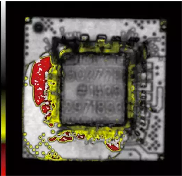
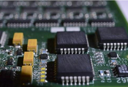
Advanced Techniques in Reliable Printed Circuit Assembly Design

Key Takeaways
Effective PCB assembly design requires balancing multiple engineering disciplines to achieve long-term reliability in demanding applications. Three core pillars emerge as critical: thermal management, signal integrity preservation, and failure-resistant layout architecture. For PCBA destined for aerospace or medical systems, adhering to IPC-6012E and MIL-PRF-31032 standards ensures compliance with rigorous environmental and operational requirements.
"A 10°C temperature rise can halve component lifespan – thermal optimization isn’t optional in high-reliability designs." – Senior Engineer, Fineline Circuits
| Technique Category | Key Metrics Improved | Industry Applications |
|---|---|---|
| Thermal Vias & Heatsinks | Junction temperature (-15°C avg.) | Automotive Power Modules |
| Differential Pair Routing | Signal Loss (<0.5dB/inch) | 5G Communication Systems |
| Conformal Coating | Moisture Resistance (IP67+) | Marine Electronics |
When selecting PCB assembly materials, prioritize high-Tg laminates (≥170°C) and low-Dk substrates for RF applications. For PCBA power distribution, implement decoupling capacitor arrays and multi-layer ground planes to mitigate voltage droop below 5%. EMI reduction strategies like guard traces and shielding cans should complement layout choices, achieving at least 30dB suppression in medical imaging systems. Always validate designs through HALT testing (-55°C to 125°C thermal cycling) and ISTM for solder joint integrity – critical steps often overlooked in prototype phases.
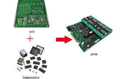
Thermal Management Strategies for PCB Reliability
Effective thermal management forms the backbone of reliable PCB assembly, particularly in applications demanding extended operational lifetimes. As component densities increase in modern high-performance electronics, heat dissipation challenges escalate, directly impacting PCBA reliability. One fundamental approach involves optimizing copper pour patterns to create low-impedance thermal paths, channeling heat away from sensitive components like processors and power modules.
Advanced PCBA designs often incorporate thermal vias—plated through-holes filled with conductive epoxy—to transfer heat between layers, paired with strategically placed heatsinks or thermal interface materials (TIMs). For mission-critical systems, such as aerospace avionics, engineers increasingly adopt embedded cooling solutions, including microchannel heat exchangers or phase-change materials, to maintain junction temperatures within safe thresholds.
Material selection also plays a pivotal role: substrates with higher glass transition temperatures (Tg) and metal-core boards provide enhanced thermal stability under cyclic loading. Simulation tools like finite element analysis (FEA) enable precise modeling of thermal gradients during PCB assembly, allowing designers to preempt hotspots before prototyping. By integrating these strategies, engineers achieve 15-30% improvements in mean time between failures (MTBF), aligning with stringent requirements for automotive and medical electronics.
Signal Integrity Enhancement in Circuit Designs
Maintaining signal integrity remains a cornerstone of reliable PCB assembly design, particularly in high-frequency applications common to aerospace and medical electronics. At the core of this challenge lies the prevention of signal distortion caused by impedance mismatches, crosstalk, or electromagnetic interference (EMI). Modern PCBA workflows employ advanced simulation tools to model transmission line behavior, enabling engineers to optimize trace geometries and dielectric materials before prototyping.
Critical techniques include controlled impedance routing, where trace widths and layer stackups are calibrated to match signal frequencies, and the strategic placement of decoupling capacitors near power-hungry components. For multi-layer boards, separating high-speed digital and analog planes with ground shielding reduces crosstalk by up to 40%, as demonstrated in recent studies. Additionally, differential pair routing with length matching ensures synchronized signal propagation, minimizing timing skew in high-speed interfaces like PCIe or DDR4.
Thermal considerations also intersect with signal integrity; uneven heat distribution in PCB assembly can alter material properties, leading to impedance drift. Integrating thermal vias near heat-generating ICs helps maintain consistent operating conditions, while low-loss laminates like Rogers 4350B preserve signal clarity across temperature fluctuations. As industries push toward miniaturization, hybrid approaches combining rigid-flex PCBA designs with embedded passive components are gaining traction, offering shorter signal paths and reduced parasitic inductance. These innovations underscore the evolving balance between performance demands and reliability in next-generation electronics.

Failure-Resistant Layout Techniques for PCBs
Designing PCB assembly layouts for failure resistance requires balancing electrical performance with mechanical robustness. A critical first step involves optimizing component placement to minimize stress concentrations, particularly in high-vibration environments common to aerospace or automotive applications. Engineers should prioritize symmetrical PCBA designs to distribute thermal and mechanical loads evenly, reducing warping risks during thermal cycling.
For signal-critical applications, trace routing strategies like avoiding 90-degree angles and implementing teardrop transitions at pad connections prevent micro-cracks and impedance discontinuities. High-current paths demand wider traces with calculated current density margins, while sensitive analog sections benefit from guard traces and Faraday cages to mitigate interference.
Incorporating redundant vias at high-stress connection points enhances reliability in multilayer boards, a practice now codified in IPC-2221B standards. Modern PCB assembly workflows leverage simulation tools to predict failure modes, enabling preemptive adjustments to pad geometries and solder mask openings.
A key advancement lies in failure mode and effects analysis (FMEA) integration during layout planning, allowing engineers to identify and mitigate risks like electrochemical migration or tin whisker formation. This approach aligns with the evolving demands of medical electronics, where PCBA reliability directly impacts patient safety.
By combining these techniques with rigorous design rule checks (DRCs), engineers create layouts that withstand accelerated aging tests while maintaining compliance with IPC-6012 Class 3 requirements for mission-critical systems.
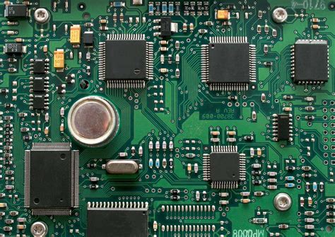
High-Reliability PCB Standards in Critical Industries
In industries where failure is not an option—such as aerospace, automotive, and medical electronics—adherence to stringent PCB assembly standards ensures operational integrity under extreme conditions. Regulatory frameworks like IPC-6012 and IPC-A-610 define Class 3 requirements for PCBA designs, mandating rigorous testing for thermal cycling, vibration resistance, and contamination control. These standards govern every phase, from material selection to final validation, ensuring boards withstand decades of use in mission-critical applications.
For example, aerospace PCB assembly protocols often specify polyimide substrates and hermetic sealing to combat rapid temperature fluctuations and moisture ingress. Medical-grade PCBA designs, meanwhile, prioritize biocompatible coatings and redundant circuitry to prevent catastrophic failures during life-saving procedures. Automotive applications demand compliance with AEC-Q100, integrating failure mode analysis into layout planning to address electromagnetic interference (EMI) risks and mechanical stress.
Building upon thermal management strategies and signal integrity enhancements, high-reliability standards enforce strict trace-width tolerances, via placement rules, and solder mask specifications. Manufacturers must also implement accelerated life testing (ALT) and environmental stress screening (ESS) to validate PCBA durability. By aligning with these benchmarks, engineers ensure that even the most complex assemblies meet the zero-defect thresholds demanded by safety-critical systems.

Advanced Material Selection for Durable PCBs
Material selection forms the cornerstone of creating PCB assembly designs that withstand harsh operational environments. Engineers increasingly prioritize substrates with high glass transition temperatures (Tg)—such as polyimide or advanced FR-4 composites—to maintain structural stability under thermal cycling. For high-frequency applications, low-loss laminates like Rogers RO4000® series minimize signal degradation while ensuring mechanical durability.
Copper weight and surface finishes also play pivotal roles in PCBA longevity. Heavy copper traces (≥3 oz) enhance current-carrying capacity and reduce thermal stress, while immersion silver or ENIG (Electroless Nickel Immersion Gold) coatings prevent oxidation and improve solder joint reliability. In mission-critical sectors like aerospace, halogen-free materials are gaining traction due to their flame-retardant properties and compliance with environmental regulations.
A common challenge in PCB assembly involves balancing material costs with performance requirements. For instance, ceramic-filled PTFE substrates offer exceptional thermal conductivity for power electronics but require specialized manufacturing techniques. To address this, designers often leverage simulation tools to model material behavior under stress, ensuring optimal choices before prototyping. For insights into mitigating material-related defects, refer to this analysis of common PCB assembly challenges.
By aligning material properties with application-specific demands—from CTE (Coefficient of Thermal Expansion) matching to moisture absorption thresholds—engineers can significantly extend the service life of PCBA systems in demanding fields like automotive electrification and medical implants.
Power Distribution Optimization in PCB Assembly
Effective power distribution forms the backbone of reliable PCB assembly, particularly in high-density designs where voltage stability directly impacts system performance. Engineers prioritize low-impedance pathways by optimizing PCBA layer stackups, strategically placing power planes, and minimizing loop inductance through symmetrical routing patterns. Modern designs often employ decoupling capacitor arrays near high-current components to suppress transient noise, while advanced simulation tools validate voltage drop thresholds across critical nodes.
For mission-critical applications like aerospace or medical devices, PCB assembly teams implement redundant power rails and copper balancing techniques to prevent localized heating. The integration of buried capacitance materials within multilayer boards further enhances power integrity by reducing parasitic effects. As noted in industry-leading practices, iterative prototyping combined with thermal-electrical co-simulation ensures robust power networks that withstand operational stressors. This approach aligns with preceding discussions on thermal management and signal integrity, creating a cohesive framework for failure-resistant layouts. By addressing current-carrying capacity during early PCBA design phases, engineers mitigate risks of electromigration and voltage sag – key factors in achieving long-term reliability across industrial and automotive electronics.
EMI Reduction Methods for Stable Electronics
Effective PCB assembly design requires meticulous attention to electromagnetic interference (EMI) mitigation, particularly in applications demanding high reliability, such as aerospace or medical electronics. A primary strategy involves optimizing grounding schemes, where multilayer PCBA layouts with dedicated ground planes minimize return path impedance. For high-frequency circuits, controlled impedance routing and differential pair configurations reduce radiated emissions by balancing signal currents.
Shielding techniques, such as incorporating Faraday cages or conductive coatings, physically isolate sensitive components from external noise. Component placement also plays a critical role—keeping high-speed traces away from analog sections and using 3D spacing rules prevents crosstalk. Additionally, decoupling capacitors placed near power pins suppress high-frequency noise in PCB assembly power distribution networks.
Advanced PCBA designs often integrate EMI filters, such as ferrite beads or common-mode chokes, to attenuate unwanted frequencies. Simulation tools like electromagnetic field solvers enable pre-production analysis of radiation patterns, allowing engineers to refine layouts before prototyping. Compliance with standards like IPC-2152 ensures designs meet industry benchmarks for EMI resilience.
By combining these methods, engineers achieve stable operation in EMI-intensive environments while maintaining compatibility with broader thermal management and signal integrity objectives outlined in earlier sections.
Validation Testing for Long-Lasting PCB Performance
Robust validation protocols form the cornerstone of ensuring PCB assembly longevity, particularly in mission-critical applications. Engineers employ accelerated life testing (ALT) to simulate years of operational stress within compressed timelines, exposing PCBA prototypes to extreme thermal cycling, vibration profiles, and humidity fluctuations. Advanced techniques like highly accelerated life testing (HALT) push designs beyond specified limits to identify failure thresholds, enabling iterative improvements before mass production.
Signal integrity validation remains paramount, with time-domain reflectometry (TDR) and vector network analysis (VNA) verifying impedance matching across high-speed traces—a critical factor often addressed during earlier design phases. For power distribution networks, in-circuit testing (ICT) validates voltage stability under load variations, while automated optical inspection (AOI) systems detect soldering defects that could compromise PCB assembly reliability.
Industry-specific standards such as IPC-6012 (Class 3) and MIL-STD-883 govern testing methodologies for aerospace and medical electronics, mandating rigorous environmental and mechanical stress evaluations. Emerging tools like AI-driven failure prediction models now complement traditional approaches, analyzing historical PCBA failure data to prioritize test scenarios. By integrating design for testability (DFT) principles early in the layout phase, teams reduce validation bottlenecks while maintaining compliance with evolving reliability benchmarks.
Conclusion
The evolution of PCB assembly techniques underscores the critical balance between innovation and reliability in modern electronics. As industries like aerospace, automotive, and medical devices demand zero-failure performance, engineers must integrate thermal optimization, signal integrity protocols, and failure-resistant layouts into every PCBA design phase. By adhering to stringent industry standards and leveraging advanced materials, designers can mitigate risks associated with power distribution anomalies and electromagnetic interference. Validation testing remains indispensable, ensuring that durable PCB assemblies meet lifecycle expectations under extreme operational stresses. Ultimately, the convergence of these methodologies not only enhances product longevity but also reinforces the trust placed in mission-critical systems. Moving forward, continuous refinement of PCBA processes will remain pivotal in addressing emerging challenges across high-stakes applications.
FAQs
How does thermal optimization affect pcb assembly reliability?
Proper thermal management in PCBA design prevents component degradation by distributing heat evenly across the board. Techniques like thermal vias and copper pours mitigate hotspots, extending the lifespan of high-power components in aerospace and automotive systems.
What design practices enhance signal integrity in dense pcb assembly layouts?
Controlled impedance routing, ground plane optimization, and minimizing crosstalk through spacing rules are critical. For PCBA in medical electronics, differential pair routing and shielding ensure stable signal transmission under electromagnetic interference (EMI).
Which standards govern failure-resistant layouts for critical industries?
Aerospace and medical PCBA must comply with IPC-6012 Class 3 and MIL-PRF-31032. These standards enforce rigorous testing for mechanical stress resistance, solder joint quality, and environmental durability.
How does material selection impact durable pcba performance?
High-Tg laminates and halogen-free substrates improve thermal stability and flame resistance. For harsh environments, ceramic-filled dielectrics reduce expansion mismatches, ensuring reliability in automotive under-the-hood applications.
Explore Professional PCB Assembly Services
For tailored solutions in high-reliability PCB assembly, please click here to consult with industry experts.


