Advancing Technology through HDI PCB Prototype Solutions

Key Takeaways
The importance of HDI PCB prototypes in modern technology is underscored by the need for advanced PCB manufacturing techniques that cater to a growing demand for compact and efficient electronic designs. You may find that PCB manufacturing companies are increasingly adopting HDI technology, which offers a range of advantages over traditional designs. For instance, the increased density of components allows for smaller circuit boards, which can be critical in industries such as telecommunications and medical technology.
While the initial investment in HDI PCB prototypes might be higher, understanding the long-term benefits can justify the PCB manufacturing cost. A detailed assessment of your project requirements can lead to significant savings when considering both production efficiency and performance upgrades. Here’s a quick comparison of key factors between traditional PCBs and HDI PCBs:
| Feature | Traditional PCBs | HDI PCBs |
|---|---|---|
| Component Density | Lower | Higher |
| Size | Bulkier | Compact |
| Data Transmission Speed | Slower | Faster |
| Manufacturing Complexity | Simpler | More complex |
As you explore these technologies, you’ll find that investing in an HDI PCB manufacturing business is not just about keeping pace with innovation; it’s about leading it. The adaptability offered by HDI solutions positions businesses like yours for sustainable growth and success in a rapidly changing technological landscape.
Understanding HDI PCB Technology: An Overview
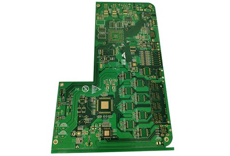
High-Density Interconnect (HDI) PCB technology is revolutionizing the realm of electronics through innovative design and functionality. This advanced method allows for the creation of more compact and efficient circuit boards, which are essential in today’s fast-paced digital landscape. By utilizing HDI PCB prototypes, your designs will not only benefit from reduced size but also from improved performance characteristics, such as enhanced signal integrity and faster data transmission speeds. As a result, HDI technology is becoming a preferred choice among PCB manufacturing companies looking to stay competitive and offer cutting-edge solutions. Understanding the nuances of HDI PCB manufacturing can empower you to make informed decisions about materials and processes, ultimately impacting the cost-effectiveness of your projects as well as their overall success. Whether you’re delving into a new product design or optimizing existing solutions, being knowledgeable about HDI capabilities will allow you to harness its potential fully while navigating the dynamic landscape of the PCB manufacturing business. This grasp not only provides a foundation for innovation but also enables you to strategically plan for future advancements in technology.
Key Advantages of HDI PCB Prototypes
HDI PCB prototypes offer a significant array of advantages that can enhance your electronic designs. One of the foremost benefits is the compact design capability, which is essential in today’s market where space optimization is crucial. This compactness allows more components to fit into smaller areas, making your designs not only more efficient but also enabling the creation of smaller yet powerful devices. Moreover, the enhanced efficiency of HDI PCBs means that they can handle higher data rates, a critical aspect in industries such as telecommunications and consumer electronics. The ability to transmit data faster opens up new possibilities for innovation in your projects.
Additionally, utilizing HDI PCB prototypes can lead to reduced overall PCB manufacturing costs, especially when scaled up for mass production. Because these manufacturing techniques allow for tighter and more precise layouts, they can decrease the material waste typically seen in standard prototype processes. By choosing reputable PCB manufacturing companies, you ensure that you’re tapping into superior craftsmanship and technology that supports your design requirements, offering quality assurance from prototype to final production.
Furthermore, as you delve into the world of electronic design, understanding the differences between traditional PCBs and HDI designs can help inform your decision-making process when selecting a PCB manufacturing business for your next project. The adoption of HDI technology not only highlights its advantages but also paves the way for meeting the increasing demands for smaller, faster, and more efficient electronic products in a competitive landscape.
Applications of HDI PCBs Across Various Industries
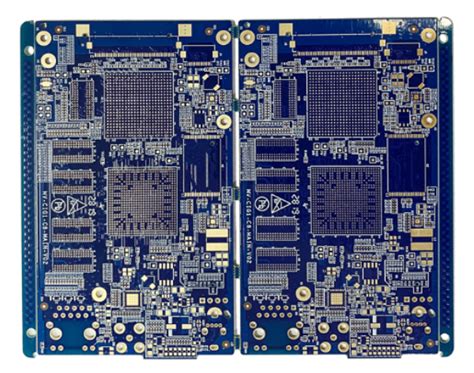
The landscape of HDI PCBs (High-Density Interconnect Printed Circuit Boards) is rapidly evolving, making significant contributions across a variety of industries. In the realm of consumer electronics, for instance, HDI PCBs are prominent in the production of smartphones and tablets, where the demand for compact design and efficient performance is paramount. By utilizing HDI PCB prototypes, companies can reduce their pcb manufacturing cost while enhancing functional density and overall product reliability. Moreover, in the healthcare sector, these advanced boards facilitate the development of sophisticated medical devices, enabling faster data transmission and improved connectivity. As your pcb manufacturing business embraces these innovations, you may find that collaborating with specialized pcb manufacturing companies that focus on HDI can lead to remarkable improvements in your product quality and market competitiveness.
"By investing in HDI technologies, you not only streamline your production processes but also elevate your innovations to meet industry challenges head-on." The automotive industry also benefits significantly from HDI technology; it is crucial for developing modern sensors and control systems that require high performance in compact spaces. As industries continue to adopt smart technologies, the versatility and efficiency of HDI PCBs will only expand further into new applications such as IoT devices, where reliability relies on the precision afforded by these advanced circuit boards. Embracing HDI PCB prototypes today can surely pave the way for your future success in a constantly evolving technological landscape.
The Development Process of HDI PCB Prototypes
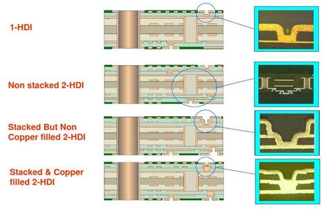
The development process of HDI PCB prototypes involves several critical steps that ensure the final product meets the demands of modern technology. To begin with, careful design considerations are paramount. Engineers utilize sophisticated software tools to create designs that maximize space while maintaining functionality, a necessity in today’s compact electronic devices. After the design phase, the next step is selecting appropriate materials that facilitate effective performance and signal integrity. This selection is particularly important as it impacts not only the efficiency of the pcb manufacturing process but also the overall pcb manufacturing cost.
Once materials are established, companies proceed with the production phase. This is where collaboration with specialized pcb manufacturing companies becomes essential, as they possess advanced capabilities to create intricate layers that define HDI technology. Utilizing techniques like laser drilling and microvias enables these companies to produce fine-featured circuit boards that traditional methods struggle to achieve. Throughout this phase, rigorous testing and evaluation occur to ensure each prototype adheres to industry standards, mitigating potential setbacks in later stages.
It’s crucial for businesses engaged in this innovative sector to maintain a keen understanding of how each step in the pcb manufacturing business contributes to the final outcome. From a conceptual design through production and testing, every element of HDI PCB development is interconnected, paving the way for technological advancements across various fields. The result? Products that not only enhance efficiency but also set new benchmarks for data transmission speeds and reliability in electronic devices worldwide.
Challenges in HDI PCB Prototype Manufacturing
Manufacturing HDI PCBs presents various challenges that can impact both the efficiency and cost-effectiveness of your PCB manufacturing endeavors. One of the major hurdles you may encounter is the complexity involved in design and fabrication. The intricate layers and fine-pitch vias utilized in HDI PCB prototypes require specialized equipment and meticulous attention to detail, making the processes significantly more sophisticated compared to traditional PCB manufacturing. Moreover, engaging with reputable PCB manufacturing companies is essential; however, not all companies have the expertise or technology to produce high-quality HDI designs, leading to variability in product quality. Additionally, the PCB manufacturing cost can escalate due to the advanced materials and technology needed for HDI circuit boards, which might affect your budget if not planned properly. Balancing performance and cost while ensuring that your prototypes meet industry standards can be a daunting task for many in the PCB manufacturing business. Adapting to these challenges proactively is crucial for leveraging the full advantages of HDI technologies in your projects.
Comparing Traditional PCBs and HDI PCBs
When evaluating traditional PCBs against HDI PCBs, it’s essential to recognize the profound impact that advancements in PCB manufacturing technologies have had on electronic design. Traditional PCB manufacturing processes often result in boards that are larger and may not efficiently accommodate the multilayer requirements needed for modern applications. In contrast, HDI PCB prototypes utilize microvias and laser-drilled holes, leading to a more compact design while retaining high performance, which is crucial for devices requiring faster data transmission.
You will find that traditional boards often struggle with heat dissipation due to their larger size, whereas HDI PCBs provide enhanced thermal management capabilities. This improvement is significant in an era where electronics are expected to operate at high speeds without overheating. Furthermore, the use of advanced materials in PCB manufacturing companies results in prototypes that support greater circuit density and improved signal integrity compared to their traditional counterparts.
While examining the pcb manufacturing cost, you may notice that the initial investment for developing HDI PCB prototypes tends to be higher due to the sophisticated technology involved, such as precision equipment and specialized materials. However, these costs are often justified by the longer-term benefits they provide, including reduced size and weight of components, leading ultimately to cost savings throughout your production cycles.
In summary, while both types serve their purposes within various applications, transitioning your projects towards utilizing HDI technology can substantially elevate both performance and innovation potential within your industry. Adopting this technology may very well represent a strategic move for your pcb manufacturing business, aligning with future trends while meeting market demands effectively.
Future Trends in HDI PCB Technology
As you look ahead in the pcb manufacturing landscape, it’s essential to consider how HDI PCB technology will evolve. The drive towards miniaturization in electronics requires that you keep pace with the increasing demand for compact and efficient components. Emerging trends indicate that pcb manufacturing companies are focusing on innovative fabrication techniques to lower pcb manufacturing costs while maintaining superior performance levels. You might find that advancements like laser drilling and advanced materials are becoming pivotal, allowing for intricate designs that were previously unattainable. Additionally, as smart devices proliferate across various sectors, the integration of HDI PCBs will be integral to enhancing data transmission speeds and efficiency. This shift not only streamlines functionality but also presents unique opportunities for you within the pcb manufacturing business sphere. Embracing these trends can not only optimize your products but also position your operations at the forefront of industry innovation, driving both performance and profitability in an increasingly competitive market.
Investing in HDI Solutions for Business Growth
As you navigate the complexities of pcb manufacturing, the decision to invest in HDI PCB solutions can significantly impact your business’s growth trajectory. The efficiency and compact design offered by HDI technology can lead to reduced pcb manufacturing costs, while enhancing performance metrics that are critical in today’s fast-paced environments. By partnering with reputable pcb manufacturing companies, you gain access to state-of-the-art design methodologies that facilitate faster data transmission and improved reliability, vital for cutting-edge applications across various sectors. Additionally, as the demand for advanced electronics ramps up, leveraging the benefits of HDI technology positions your pcb manufacturing business at the forefront of innovation. Adopting these solutions not only aligns with industry trends but also streamlines your production processes, enabling you to meet customer needs with agility and precision. Investing in HDI solutions is not merely a technical upgrade; it’s a strategic move that fosters sustainable growth and drives your business forward in an increasingly competitive marketplace.
Conclusion
In the ever-evolving landscape of technology, HDI PCB prototypes stand out for their ability to push the boundaries of what is possible in electronic design. As you consider the impact of HDI PCBs, it is essential to recognize their role in redefining pcb manufacturing practices. These prototypes not only support compact designs but also enhance data transmission speeds, making them a favorite among pcb manufacturing companies looking to stay competitive. The efficiency and performance offered by HDI PCBs can significantly influence your pcb manufacturing business, ultimately leading to a reduction in pcb manufacturing costs through optimized material usage and minimized space requirements. Embracing this technology helps pave the way for innovation across various sectors, ensuring that your products remain at the forefront of industry standards. As you explore opportunities within this domain, keep in mind that investing in HDI solutions could be key to unlocking future growth and technological advancement in your pcb manufacturing endeavors.
FAQs
What are HDI PCBs?
HDI (High-Density Interconnect) PCBs are advanced printed circuit boards designed with a higher density of components and connections, which allows for more compact and efficient designs. They cater to the growing demand for smaller electronics without compromising performance.
How does HDI PCB manufacturing differ from traditional PCB manufacturing?
The pcb manufacturing process for HDI PCBs incorporates finer lines, smaller pads, and multiple layers, enabling higher density layouts. This results in enhanced connectivity and improved thermal management compared to traditional PCBs, which typically have larger traces and spaces.
What industries benefit from HDI PCB prototypes?
Various industries such as consumer electronics, telecommunications, automotive, and medical devices leverage HDI PCB prototypes. These prototypes allow companies to test new designs rapidly while maintaining pcb manufacturing cost effectiveness, leading to faster innovation cycles.
Are there specific challenges associated with HDI PCB prototype manufacturing?
Yes, the complexity of HDI PCBs demands advanced skills and technology in the fabrication process. Common challenges include alignment accuracy during multilayer assembly and ensuring signal integrity due to the increased density of pathways.
What should I consider before choosing a PCB manufacturing company for HDI projects?
When selecting a pcb manufacturing company, consider their expertise in HDI technology, the quality control measures in place, lead times for prototype production, and cost structures. Understanding these factors can greatly impact your overall project success.
For more information about how to effectively engage with HDI solutions for your business growth, please click here: Andwin PCB Manufacturing


