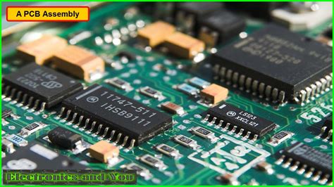
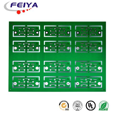
Advantages of Multilayer PCB Prototypes for Advanced Designs
Key Takeaways
When considering multilayer PCB prototypes, you will discover that they offer several significant advantages in the realm of PCB manufacturing. One of the most compelling benefits is the enhanced performance that these PCBs deliver. By allowing for more complex circuit layouts, multilayer designs enable you to fit more functionality into a smaller footprint, which is particularly beneficial for advanced electronic applications. This translates to a reduction in overall size and weight of your devices while maintaining or even increasing their efficiency.
Moreover, multilayer PCBs significantly reduce electromagnetic interference, a critical factor in ensuring reliable operation in sensitive electronics. When you’re dealing with intricate designs, the ability to effectively manage interference becomes essential. This is where working with skilled PCB manufacturing companies can make a notable difference, as they can provide tailored solutions that meet your specific requirements.
Engaging with these manufacturers also allows you to conduct a thorough cost-benefit analysis of multilayer versus standard PCBs. Although there might be an initial rise in PCB manufacturing costs, the long-term reliability and performance enhancements justify the investment for many projects. Ultimately, embracing multilayer PCB prototypes can facilitate innovation while ensuring that your projects not only meet industry standards but also push the boundaries of what’s possible in modern electronics.
“Investing in quality PCB design can lead to superior performance and reliability; don’t compromise on this aspect.”
Introduction to Multilayer PCB Prototypes
When embarking on a project requiring advanced designs, understanding the role of multilayer PCB prototypes in the realm of pcb manufacturing is essential. These prototypes are not just a new trend; they represent a significant evolution in circuit board technology. By leveraging multiple layers, you can achieve enhanced performance that single or double-layer PCBs simply cannot offer. This complexity allows you to create more compact designs, which is crucial when space and efficiency are paramount considerations.
In your journey through the world of pcb manufacturing companies, it’s vital to recognize that the initial pcb manufacturing cost for multilayer prototypes may be higher. However, this investment is often offset by the long-term benefits of reliability and functionality they provide in your electrical designs. With multilayer prototypes, you can minimize electromagnetic interference, which can adversely affect signal integrity if not addressed effectively. This attribute ensures that your products perform well even under challenging conditions.
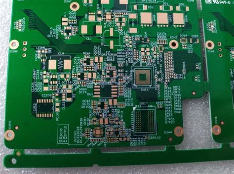
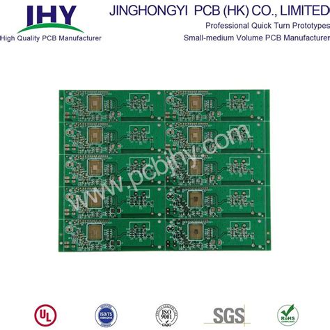
Moreover, multilayer configurations enable you to accommodate complex circuit layouts that simply wouldn’t fit within traditional standards. You gain access to intricate connections without sacrificing space or quality, making these prototypes essential for industries requiring specialized and sophisticated applications. The tables below encapsulate some defining differences between multilayer and standard PCBs, illustrating how they play a critical role in various sectors:
| Feature | Multilayer PCBs | Standard PCBs |
|---|---|---|
| Layer Count | 3 or more | 1-2 |
| Space Efficiency | High | Moderate |
| Signal Integrity | Excellent | Good |
| Manufacturing Complexity | Higher | Lower |
| Typical Applications | Medical devices, aerospace | Basic consumer electronics |
Overall, investing time and resources into understanding how multilayer PCB prototypes enhance design capabilities is invaluable for any aspiring professional within the pcb manufacturing business. These boards are not just about meeting technical requirements but also about setting new standards for innovation and quality within the industry.
Enhanced Performance of Multilayer PCBs
When you consider multilayer PCB prototypes, one of the most significant benefits is the enhanced performance they provide. These prototypes allow for a higher density of components within a smaller footprint, thus enabling the creation of complex circuit designs that are not feasible with standard PCBs. This is particularly beneficial in applications where space is at a premium, like in portable electronics or medical devices. Additionally, multilayer designs allow for improved routing of signals, reducing the distance that electrical signals must travel and ultimately resulting in faster overall performance.
Moreover, as technology evolves, demands for higher frequencies and lower power consumption grow. With multilayer configurations, you can achieve a better arrangement for power and ground layers, minimizing the impact of parasitic capacitance and enhancing signal integrity. This capability directly influences pcb manufacturing processes, as manufacturers need to adapt their techniques to maintain quality across multiple layers. By working with reputable pcb manufacturing companies, you can ensure that these intricate designs not only perform well but also remain consistent throughout their lifecycle.
It’s critical to consider that while multilayer PCBs often come with a higher pcb manufacturing cost, the advantages they offer in terms of reliability and performance can lead to reduced costs down the line due to fewer failures and less need for troubleshooting. Therefore, understanding how multilayer PCB prototypes enhance performance can assist you in making informed decisions about your projects, especially as you weigh the cost-benefit analysis against simpler designs in your pcb manufacturing business.
Reducing Electromagnetic Interference in Design
In the realm of multilayer PCB prototypes, reducing electromagnetic interference (EMI) is essential for achieving optimal performance in your designs. By utilizing a multilayer structure, you can strategically arrange signal layers and ground planes, which helps to shield sensitive traces from external noise sources. This arrangement not only minimizes the risk of interference but also enhances the overall reliability of the circuit. Additionally, incorporating proper spacing and using high-quality materials during the PCB manufacturing process plays a crucial role in further mitigating EMI problems. Selecting reputable pcb manufacturing companies will ensure that you receive prototypes designed with advanced techniques that adhere to industry standards. As a result, investing in multilayer PCB prototypes may initially appear to increase your overall pcb manufacturing cost, but the long-term benefits—like improved device performance and reduced troubleshooting time—can provide significant savings for your pcb manufacturing business. By carefully considering these factors, you can effectively create designs that not only meet your specifications but also excel under various operational conditions.
Complex Circuit Layouts: Benefits and Solutions
In today’s rapidly evolving technological landscape, the demand for multilayer PCB prototypes continues to rise, particularly when it comes to implementing complex circuit layouts. These prototypes allow you to effectively manage an increasing number of components while ensuring that your designs remain compact and efficient. One of the primary benefits of utilizing multilayer PCBs is their inherent capability to enhance signal integrity and reliability. By layering circuits, you reduce the length of connections between components, which minimizes potential signal degradation. Furthermore, multilayer configurations provide a thoughtful approach to managing electromagnetic interference (EMI), shielding sensitive areas of your design from external sources of disruption.
Leveraging the expertise of experienced PCB manufacturing companies, you can capitalize on advanced techniques and materials specifically tailored for high-density interconnects. This not only achieves superior performance but also facilitates innovative designs that meet rigorous industry standards. Although the PCB manufacturing cost may be higher than traditional methods, the efficiency gained in terms of size and performance provides significant returns on investment over time. As a result, your PCB manufacturing business can flourish in competitive markets by delivering products that enhance functionality and reliability through sophisticated design solutions. Emphasizing these advantages positions your projects at the forefront of technology, allowing you to tackle even the most demanding applications with confidence.
Ensuring Reliability in Advanced PCB Designs
When it comes to multilayer PCB prototypes, ensuring reliability in your designs is crucial. Advanced electronic devices demand high performance, and multilayer PCBs are designed to meet these challenges head-on. By incorporating multiple layers, you can effectively distribute the electrical signals across various pathways, which minimizes the risk of circuit failure. This is particularly beneficial when you consider factors like temperature fluctuation and mechanical stress that can affect performance.
Moreover, the robust nature of multilayer PCBs allows for integration of complex circuit layouts without compromising on quality. You may also notice a marked reduction in signal degradation compared to conventional designs, leading to consistent and reliable functionality in your projects. Additionally, partnering with reputable pcb manufacturing companies can help ensure that your prototypes are crafted with precision, utilizing advanced techniques and high-quality materials that enhance durability.
It’s essential to recognize that although there may be a higher pcb manufacturing cost associated with multilayer designs compared to standard options, the long-term benefits often outweigh this initial expenditure. From reducing maintenance issues to enhancing device longevity and performance, these prototypes can significantly elevate your project’s reliability metrics. In a competitive pcb manufacturing business, choosing multilayer solutions can set your work apart by demonstrating a commitment to quality and innovation in design.
Cost-Benefit Analysis of Multilayer vs. Standard PCBs
When considering multilayer PCB prototypes, it is crucial to conduct a thorough cost-benefit analysis compared to standard PCBs. While the initial pcb manufacturing cost for multilayer designs may be higher, the long-term advantages can significantly outweigh the initial investment. For instance, multilayer PCBs can accommodate more complex designs, leading to reduced space requirements and potentially lower production costs over time. Moreover, pcb manufacturing companies often highlight that multilayer boards improve performance efficiency and reliability through enhanced signal integrity. This is particularly important in advanced electronic devices that demand compact layouts with minimal electromagnetic interference. You may find that by investing in a multilayer PCB prototype, your pcb manufacturing business can gain a competitive edge due to improved product reliability and enhanced operational performance. Ultimately, choosing the right type of PCB hinges on your specific design requirements and the desired longevity of your electronic products, making it vital for you to weigh both the upfront costs and potential benefits before making a decision.
Applications of Multilayer PCBs in Various Industries
The versatility of multilayer PCBs makes them an integral component across numerous industries. In telecommunications, for instance, these advanced boards are pivotal for managing high-frequency signals and ensuring clear communication. Their ability to minimize electromagnetic interference allows companies to produce reliable devices that can withstand temporal noise, thereby improving overall performance. In the realm of medical devices, multilayer PCBs play a crucial role in ensuring the precision and reliability required for critical applications such as diagnostic equipment and patient monitoring systems. Furthermore, industries involved in automotive design have adopted multilayer technology to support the complex electronics needed for modern vehicles, enhancing functionality while meeting stringent safety standards. As you explore pcb manufacturing options, consider the importance of these prototypes in streamlining your designs and meeting the demands of advanced applications. By partnering with reputable pcb manufacturing companies, you can benefit from tailored solutions that cater to your specific needs, ultimately impacting your project’s success positively. While analyzing the associated pcb manufacturing cost, it’s essential to recognize that investing in multilayer designs may lead to long-term efficiencies and superior product outcomes. With a solid grasp of how multilayer PCBs serve various sectors, you can make informed decisions that align with your projects’ objectives and challenges encountered within the ever-evolving technological landscape.

Conclusion
In summary, multilayer PCB prototypes play an essential role in the evolution of modern electronic designs. By opting for these advanced circuit boards, you can significantly enhance the overall performance of your projects. The integration of multiple layers allows for a more sophisticated design layout, enabling you to implement intricate functionalities without increasing the size of your device. Furthermore, multilayer PCBs are engineered to minimize electromagnetic interference (EMI), which is critical in maintaining signal integrity in high-frequency applications.
When it comes to reliability, multilayer boards are designed to withstand demanding operational environments, thus supporting long-term performance and durability. This reliability is paramount for industries that rely on complex circuit fabrication and high-precision electronics, as it reduces the frequency of failures and subsequent costs. Speaking of costs, while there may be a higher initial pcb manufacturing cost compared to standard options, the benefits often outweigh these expenses. With reduced assembly time and fewer components required due to improved design capabilities, working with reputable pcb manufacturing companies can result in substantial savings in your overall pcb manufacturing business strategy.
Ultimately, embracing multilayer PCB prototypes not only paves the way for complex layouts but also ensures that your electronic products can compete effectively in today’s fast-paced technological landscape. By understanding and leveraging these advantages, you position yourself well within your industry while driving innovation and efficiency in your projects.
FAQs
What are multilayer PCB prototypes?
Multilayer PCB prototypes consist of multiple conductive layers that are stacked and laminated together, allowing for more complex circuit layouts compared to standard PCBs.
How do multilayer PCBs enhance performance?
They enhance performance by providing better electrical routing, which can significantly improve signal integrity and speed in advanced electronic designs.
Can multilayer PCBs reduce electromagnetic interference (EMI)?
Yes, multilayer designs can help in reducing electromagnetic interference by allowing for tighter signal control and shielding through strategic layer placement. This is crucial for maintaining the functionality of sensitive components.
What are the benefits of complex circuit layouts in multilayer PCBs?
Complex circuit layouts enable you to pack more functionality into a smaller space, which is essential for modern devices that require compact designs without sacrificing performance.
How do multilayer PCBs ensure reliability?
With improved thermal management and mechanical stability, multilayer PCBs ensure reliability through enhanced durability and performance consistency across varied conditions.
What is the cost comparison between multilayer and standard PCBs?
While the initial pcb manufacturing cost may be higher for multilayer boards due to their complexity, they often result in overall savings by reducing surface area and improving device performance.
What industries utilize multilayer PCBs?
Multilayer PCs are widely used across various industries including telecommunications, automotive, aerospace, and consumer electronics due to their versatility and efficiency in design.
If you’re interested in exploring how pcb manufacturing companies can help you create high-quality prototypes, please visit this link.