Aerospace Grade PCBs: Design, Materials, and Manufacturing for Extreme Environments
Introduction to Aerospace PCBs
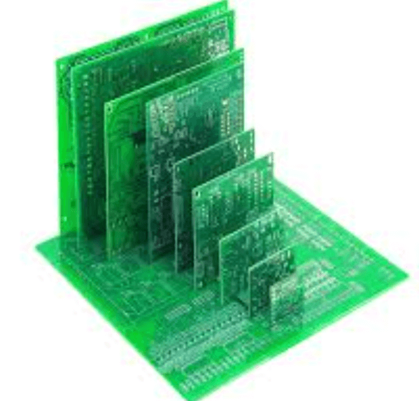
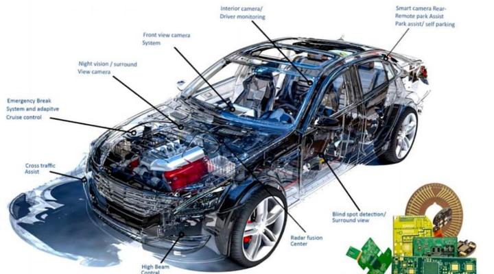
Printed Circuit Boards (PCBs) form the backbone of modern aerospace electronics, serving critical functions in avionics, navigation systems, communications equipment, and flight control systems. Aerospace grade PCBs differ significantly from their commercial counterparts due to the extreme environmental conditions they must endure while maintaining flawless operation. These specialized circuit boards must withstand temperature extremes, intense vibration, mechanical stress, radiation, and other harsh conditions while providing absolute reliability—human lives and multi-million dollar equipment depend on their flawless performance.
The aerospace PCB market has grown substantially in recent years, projected to reach $XX billion by 2025, driven by increasing aircraft production, satellite deployments, and defense spending. This article explores the unique requirements, materials, design considerations, manufacturing processes, and testing protocols that distinguish aerospace grade PCBs from commercial-grade boards.
Extreme Environmental Requirements
Aerospace PCBs operate in some of the most demanding environments imaginable, requiring careful engineering to ensure reliability under these extreme conditions:
Temperature Extremes: Aerospace electronics must function across a staggering temperature range. High-altitude aircraft experience ambient temperatures from -55°C to +85°C, while space applications can see extremes from -150°C in shadow to +150°C in direct sunlight. PCBs must maintain structural integrity and electrical performance throughout these ranges, with some specialized applications requiring operation up to 200°C or higher for engine-mounted electronics.
Mechanical Stress: Vibration is a constant challenge in aerospace applications. Aircraft experience vibration frequencies from 10Hz to 2000Hz with significant G-forces, while rocket launches subject electronics to intense acoustic vibration (up to 150dB) and mechanical shock (up to 100G). PCBs must be designed to resist these forces without developing cracks or intermittent connections.
Outgassing: In space applications, materials must minimize outgassing—the release of trapped gases in vacuum conditions—which can contaminate optical surfaces or sensitive instruments. NASA and ESA maintain strict outgassing standards (typically <1% total mass loss and <0.1% collected volatile condensable materials).
Radiation: Space electronics face ionizing radiation that can cause single-event upsets (SEUs), latch-up, or total dose effects. Aerospace PCBs often incorporate radiation-hardened materials and designs to mitigate these effects.
Altitude and Pressure: Rapid pressure changes can cause delamination or “popcorning” in poorly constructed PCBs. Aerospace boards must withstand pressure variations from sea level to near-vacuum conditions.
Materials Selection for Aerospace PCBs
The substrate materials used in aerospace PCBs differ significantly from standard FR-4 used in commercial applications. Key material considerations include:
High-Temperature Laminates:
- Polyimide: The most common aerospace PCB material, offering excellent thermal stability (continuous operation up to 260°C), low CTE, and good mechanical properties. Popular grades include Dupont’s Kapton and Rogers’ polyimide materials.
- PTFE (Teflon): Used for high-frequency applications due to its excellent dielectric properties, though more challenging to manufacture.
- Ceramic-filled PTFE: Combines PTFE’s electrical properties with improved thermal conductivity and mechanical stability.
- Aluminum and Copper Clad: For high-power applications requiring heat dissipation.
Copper Foil:
- Heavy copper (up to 20oz) for high-current applications
- Electrodeposited copper with high elongation for improved thermal cycling performance
- Reverse-treated foil for better adhesion in extreme conditions
Surface Finishes:
- Electroless Nickel Immersion Gold (ENIG): Most common aerospace finish, providing good solderability and wire bondability
- Immersion Silver: For high-frequency applications
- Electrolytic Hard Gold: For connectors and high-wear areas
- Organic Solderability Preservatives (OSP): Limited to less critical applications
Specialty Materials:
- Low-outgassing adhesives and solder masks
- Radiation-shielding materials (tungsten or tantalum filled) for space applications
- Nanocomposite materials for improved thermal and mechanical properties
Design Considerations for Aerospace PCBs
Aerospace PCB design follows rigorous standards (IPC-6012 Class 3/3A, MIL-PRF-31032, MIL-PRF-55110) with additional requirements:
High-Reliability Layout:
- Conservative design rules with wider traces and spaces
- Redundant vias and connections for critical signals
- Avoidance of single-point failures
- Proper creepage and clearance for high-voltage applications
Thermal Management:
- Careful component placement to avoid hot spots
- Thermal relief patterns for even heat distribution
- Incorporation of thermal vias and heat sinks
- Consideration of thermal expansion mismatches
Signal Integrity:
- Controlled impedance for high-speed signals
- Careful routing to minimize crosstalk and EMI
- Proper grounding strategies (often multi-point in aerospace)
- Shielding for sensitive circuits
Mechanical Robustness:
- Reinforced board edges and mounting holes
- Strategic stiffener placement
- Conformal coating considerations in layout
- Component selection and placement to withstand vibration
Testability:
- Incorporation of test points for in-circuit testing
- Boundary scan (JTAG) implementation
- Built-in self-test (BIST) circuits for critical functions
Manufacturing Processes for Aerospace PCBs
Aerospace PCB manufacturing follows exacting standards with rigorous process controls:
Fabrication Process:
- Material certification and traceability
- Precision drilling (mechanical and laser)
- Plasma desmear for high-reliability plated through holes
- Direct metallization or chemical copper processes
- Electrolytic copper plating with tight thickness control
- Advanced imaging (LDI for fine features)
- Etching with process controls to prevent over-etch
- Automated optical inspection (AOI) at multiple stages
- Electrical testing (100% continuity and isolation)
- Controlled lamination processes for multilayer boards
Special Processes:
- Sequential lamination for complex multilayer boards
- Embedded components technology
- Microvia and HDI technology for high-density designs
- Special via treatments (tented, plugged, or filled vias)
- Conformal coating application (parylene, acrylic, or silicone)
Quality Control:
- Full material traceability (lot codes, certifications)
- Process control documentation
- Microsection analysis for via quality
- Solderability testing
- Ionic contamination testing
Testing and Qualification
Aerospace PCBs undergo extensive testing to verify reliability:
Electrical Testing:
- 100% electrical test (continuity and isolation)
- Impedance testing for controlled impedance boards
- High-potential (hipot) testing
- Time-domain reflectometry (TDR) for signal integrity verification
Environmental Testing:
- Thermal cycling (-55°C to +125°C minimum, often more extreme)
- Vibration testing (random and sine vibration profiles)
- Mechanical shock testing
- Humidity and moisture resistance testing
- Outgassing testing (for space applications)
Long-Term Reliability Testing:
- Highly Accelerated Life Testing (HALT)
- Highly Accelerated Stress Screening (HASS)
- Temperature-humidity-bias (THB) testing
- Interconnect stress testing (IST)
Certifications and Standards:
- IPC-6012 Class 3/3A
- MIL-PRF-31032 (replaces MIL-P-55110)
- MIL-PRF-50884 for flexible circuits
- NASA/SMAP specifications for space applications
- ESA ECSS standards for European space projects
- DO-160 for airborne equipment environmental conditions
Emerging Technologies in Aerospace PCBs
The aerospace PCB industry continues to evolve with new technologies:
Advanced Materials:
- Nanocomposite substrates with improved thermal and mechanical properties
- Low-loss, low-Dk materials for millimeter-wave applications (5G, radar)
- Embedded passive and active components
Manufacturing Innovations:
- Additive manufacturing of PCBs
- 3D printed electronics
- Laser direct structuring (LDS) for three-dimensional circuits
- Advanced embedded component technology
Design Innovations:
- AI-assisted design for reliability optimization
- Model-based engineering (MBE) approaches
- Digital twin technology for predictive maintenance
Sustainability Initiatives:
- Lead-free and halogen-free materials
- Recyclable substrate materials
- Reduced chemical usage processes
Challenges and Future Directions
The aerospace PCB industry faces several challenges:
Supply Chain Issues:
- Limited sources for high-reliability materials
- Long lead times for specialty components
- Counterfeit component prevention
Technological Challenges:
- Managing increasing complexity while maintaining reliability
- Meeting higher frequency requirements (mmWave, THz)
- Integrating more functionality in smaller form factors
Cost Pressures:
- Balancing extreme reliability requirements with cost constraints
- Justifying the premium for aerospace-grade versus commercial-off-the-shelf (COTS)
- Lifecycle cost versus initial cost considerations
Future developments will likely focus on:
- Further miniaturization while maintaining reliability
- Improved thermal management techniques
- More robust radiation hardening for space applications
- Integration of more AI and machine learning capabilities
- Development of more sustainable materials and processes
Conclusion
Aerospace grade PCBs represent the pinnacle of printed circuit board technology, combining advanced materials, precision engineering, and rigorous testing to create electronics capable of surviving the most extreme environments imaginable. As aerospace systems become more complex and demanding, the requirements for these critical components will only increase. Manufacturers and designers must continue to innovate while maintaining the uncompromising standards that make aerospace electronics uniquely reliable. The future of aerospace PCBs lies in balancing these extreme reliability requirements with emerging technologies and the constant pressure for improved performance in smaller, lighter packages.