Altium Designer Tutorial: A Comprehensive Guide for Beginners
Introduction to Altium Designer
Altium Designer is one of the most powerful and widely-used electronic design automation (EDA) software tools in the industry today. Developed by Altium Limited, this integrated solution provides PCB designers with all the necessary tools to create complex printed circuit boards (PCBs) from concept to manufacturing. Whether you’re a hobbyist working on personal projects or a professional engineer designing cutting-edge electronics, mastering Altium Designer can significantly enhance your productivity and design capabilities.
This comprehensive tutorial will guide you through the fundamental aspects of Altium Designer, including:
- The user interface and basic navigation
- Schematic capture and component management
- PCB layout design and routing techniques
- Design rule checking and validation
- Output generation for manufacturing
Getting Started with Altium Designer
Installation and Setup
Before diving into design work, you’ll need to properly install and configure Altium Designer:
- Download the installer from Altium’s official website
- Follow the installation wizard, selecting appropriate components
- Activate your license (student, trial, or commercial)
- Configure preferences under Preferences > System > General
- Set up your default workspace and panel layout
Understanding the User Interface
Altium Designer’s interface consists of several key components:
- Menu Bar: Contains all major commands organized by function
- Toolbars: Quick access to frequently used tools (customizable)
- Projects Panel: Displays your current project hierarchy
- Workspace: Main area for schematic and PCB editing
- Panels: Various supporting panels like Properties, Libraries, and Messages
Tip: Use View > Workspace Panels to show/hide specific panels as needed for your workflow.
Schematic Design Fundamentals
Creating a New Schematic
- File > New > Project > PCB Project
- Right-click project > Add New to Project > Schematic
- Save your project with a meaningful name
Working with Components
Placing Components:
- Use Place > Part or the shortcut P,P
- Search for components in available libraries
- Place components with appropriate orientation
Component Properties:
- Double-click any component to edit its properties
- Pay special attention to designator (reference designator) and comment (value)
- Define footprint associations for PCB layout
Wiring Your Schematic
- Use Place > Wire or the shortcut P,W
- Connect component pins according to your circuit design
- Use nets and net labels for complex connections
- Add power ports (VCC, GND) using Place > Power Port
Schematic Best Practices
- Use a logical flow from inputs to outputs
- Group related components together
- Add clear labeling and documentation
- Use hierarchical sheets for complex designs
- Perform regular consistency checks (Tools > Schematic Check)
PCB Design Essentials
Transitioning from Schematic to PCB
- Design > Update PCB Document (or Create PCB from Schematic)
- Review the Engineering Change Order (ECO) for accuracy
- Execute changes to import components and nets
Board Setup and Stackup
- Define your board shape (Design > Board Shape)
- Configure layer stack (Design > Layer Stack Manager)
- Set appropriate design rules (Design > Rules)
- Clearance constraints
- Routing widths
- Via styles
- Manufacturing requirements
Component Placement Strategies
- Start with critical components (connectors, processors)
- Group related components together
- Consider thermal management and signal integrity
- Use alignment tools for professional layouts
- Leave adequate space for routing
Routing Techniques
Manual Routing:
- Route > Interactive Routing (shortcut P,T)
- Use Shift+Space to cycle through corner styles
- Press * to change layers (automatically inserts via)
Auto-Routing:
- Route > Auto Route > All
- Configure routing strategies as needed
- Typically requires manual cleanup
Advanced Routing Features:
- Differential pair routing
- Length tuning
- Interactive length tuning
- Teardrops (Tools > Teardrops)
Copper Pour and Planes
- Place > Polygon Pour
- Define net association and pour settings
- Use plane layers for power distribution
- Configure polygon connect styles
Design Verification and Output
Design Rule Checking (DRC)
- Tools > Design Rule Check
- Configure check options
- Run DRC and review violations
- Address all critical violations before manufacturing
Generating Manufacturing Outputs
Gerber Files:
- File > Fabrication Outputs > Gerber Files
- Configure layers and options
- Generate and review
Drill Files:
- File > Fabrication Outputs > NC Drill Files
- Configure drill options
- Generate and review
Bill of Materials (BOM):
- Reports > Bill of Materials
- Configure columns and formatting
- Export in desired format (Excel, CSV, PDF)
Assembly Drawings:
- File > Assembly Outputs > Assembly Drawings
- Configure views and layers
- Generate PDF or other formats
Advanced Features and Tips
Library Management
- Create and manage component libraries
- Use the Component Library Editor
- Develop a consistent library strategy
- Consider using managed content servers
Version Control Integration
- Set up version control (Preferences > Version Control)
- Use SVN or Git integration
- Commit regularly with meaningful comments
Scripting and Automation
- Explore Altium’s scripting capabilities
- Use Delphi or JavaScript for custom scripts
- Automate repetitive tasks
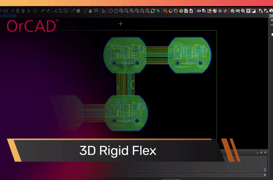
3D Visualization
- View > 3D Layout Mode
- Import mechanical components
- Check for mechanical conflicts
Common Pitfalls and Troubleshooting
- Footprint Mismatches: Always verify footprint associations
- Unrouted Nets: Double-check all connections in schematic and PCB
- DRC Violations: Don’t ignore design rule violations
- Manufacturing Issues: Always review output files before sending to fabrication
- Performance Problems: Break large designs into smaller blocks when possible
Learning Resources and Next Steps
To continue your Altium Designer education:
- Official Documentation: Altium’s comprehensive help system
- Video Tutorials: Altium’s YouTube channel and training portal
- Community Forums: Engage with other designers
- Training Courses: Consider formal certification programs
- Practice Projects: Start with simple designs and gradually increase complexity
Conclusion
Altium Designer is a sophisticated tool with capabilities that extend far beyond this introductory tutorial. As you become more comfortable with the basics presented here, you’ll discover advanced features that can further streamline your design workflow and improve your PCB quality. Remember that mastery comes with practice, so don’t hesitate to experiment with personal projects and explore the software’s extensive capabilities.
By following this tutorial and continuing your learning journey, you’ll be well on your way to becoming proficient in one of the electronics industry’s most powerful design tools. Whether you’re designing simple Arduino shields or complex multilayer boards, Altium Designer provides the tools you need to bring your electronic concepts to life.

