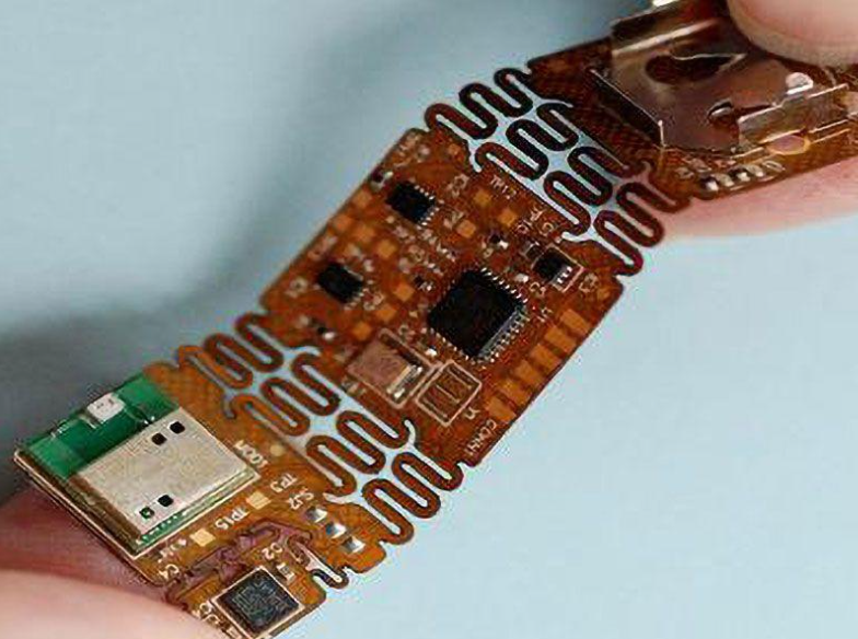
altium flex pcb bending
Best Practices for Designing Flexible Circuit Boards
When designing flexible circuit boards (Flex PCBs), following best practices is key to ensuring their performance and reliability. First, choosing the right material is critical. Polyimide is the most commonly used substrate because of its excellent thermal stability and mechanical strength. In addition, the thickness of the copper foil also needs to be carefully considered. Thinner copper foil can improve flexibility but may affect conductive properties. Therefore, designers need to find a balance between flexibility and electrical performance.
Next, wiring design is another important aspect. To reduce stress concentration, it is recommended to use rounded corners instead of right angles. Right angles can create stress concentration when bending, which may cause copper foil to break. In addition, the width and spacing of the wiring also need to be carefully planned. Wider wiring can disperse stress, but may take up more space. Therefore, designers need to balance space utilization and stress dispersion.
In addition, the design of vias also requires special attention. Vias are one of the most fragile parts of the circuit board, especially in the bending area. To improve the reliability of vias, it is recommended to use filled vias or blind via designs. These designs can reduce stress concentration and thus improve the durability of the circuit board.
During the design process, it is also crucial to consider the bending radius. Too small a bending radius will increase the stress of the circuit board, which may cause breakage or performance degradation. Generally speaking, the bending radius should be at least ten times the thickness of the circuit board. In addition, the wiring in the bending area should be minimized to reduce stress concentration.
To further improve the reliability of the design, it is recommended to use reinforcement materials in the bending area. Reinforcement materials can disperse stress and reduce the risk of breakage. Commonly used reinforcement materials include glass fiber and polyimide film. These materials can not only improve the mechanical strength of the circuit board, but also improve its thermal stability.
Finally, testing and verification are key steps to ensure the success of the design. Before production, simulation and physical testing can help identify potential problems. Through tools such as finite element analysis (FEA), you can simulate the performance of the board under different conditions to optimize the design. In addition, physical testing can verify the simulation results to ensure the reliability of the board in actual applications.
In summary, designing flexible circuit boards requires comprehensive consideration of multiple factors such as material selection, routing design, via design, bend radius, and reinforcement materials. By following these best practices, the performance and reliability of the board can be significantly improved to meet various application needs.
Bend Region Setup Tips in Altium
When designing Flexible Printed Circuit Boards (Flex PCBs), Altium Designer provides a range of powerful tools and features to help engineers implement complex bend region setups. First, it is crucial to understand how to define and manage bend regions in Altium. By using bend region setups, designers can precisely control the degree of bend in different parts of the board, ensuring that the board will work properly in the actual application.
To begin setting up bend regions, designers need to create a new flex PCB project in Altium. Next, use the “Layer Stack Manager” tool to define the layer stackup structure of the board. This tool allows designers to specify which layers are flexible and which are rigid. In this way, a rigid-flex design can be achieved on the same board to meet the needs of different application scenarios.
After defining the stackup structure, designers can use the “Region” tool to divide the board into different areas. By drawing regions in the PCB design interface, designers can specify which parts are bending areas and which parts are rigid areas. Next, use the “Bend Line” tool to add bend lines in the bend area. The setting of the bend line is very important because it directly affects the bend radius and bend angle of the board. By accurately setting the bend line, designers can ensure that the board will not be damaged or fail when bent.
In addition, Altium also provides a “Bend Radius” setting option that allows designers to specify the minimum bend radius of the bend area. This setting is critical to ensuring the reliability of the board, because a too small bend radius may cause the board to break or damage the conductive path. By setting the bend radius reasonably, designers can ensure the structural integrity of the board while ensuring the flexibility of the board.
After completing the setting of the bend area and bend line, designers can use Altium’s 3D view function to preview the bending effect of the board. Through the 3D view, designers can intuitively see the shape of the circuit board after bending, so as to make necessary adjustments and optimizations. This function not only improves the accuracy of the design, but also greatly reduces the trial and error costs in actual production.
In short, Altium Designer provides a series of powerful tools and functions to help designers realize complex flexible circuit board design. By reasonably setting the bending area, bending line and bending radius, designers can ensure that the circuit board has good flexibility and reliability in actual applications. Using Altium’s 3D view function, designers can also intuitively preview and optimize the design, thereby improving design efficiency and accuracy. With these techniques, designers can better cope with various challenges in flexible circuit board design and create high-quality products.
How to simulate the bending of flexible PCB in Altium
In modern electronic design, flexible printed circuit boards (Flex PCBs) are widely used in various high-tech devices due to their flexibility and adaptability. In order to ensure the reliability and functionality of the design, it becomes crucial to simulate the bending behavior of flexible PCBs. As a powerful electronic design automation tool, Altium Designer provides a variety of functions to help engineers achieve this goal.
First of all, understanding the basic characteristics of flexible PCBs is a prerequisite for simulating bending behavior. Flexible PCBs are composed of multiple layers of thin film materials with good bending performance and durability. In Altium, designers can accurately simulate these properties by defining material properties and stacking structures. By setting the elastic modulus and Poisson’s ratio of the material, the physical behavior of the flexible PCB when bent can be more realistically reflected.
Next, creating a 3D model is one of the key steps in simulating the bending of a flexible PCB. Altium Designer provides powerful 3D modeling capabilities that allow designers to view and manipulate PCBs in three-dimensional space. By importing or creating a 3D model, designers can intuitively observe the morphological changes of the PCB at different bending angles. This not only helps to verify the feasibility of the design, but also discover potential problems in advance.
After the 3D model is created, simulation using Altium’s bending simulation tool is the next step. By setting the bending radius and bending angle, designers can simulate the bending effect under different conditions. Altium’s simulation tool can display the distribution of stress and strain during bending in real time, thereby helping designers optimize the design and avoid fracture or failure due to excessive bending.
In addition, Altium also provides interfaces with other simulation software to further enhance the accuracy and reliability of flexible PCB bending simulation. For example, through integration with finite element analysis software such as ANSYS, designers can perform more detailed mechanical analysis to ensure the stability and durability of the design in practical applications.
Finally, verification and optimization are the final steps of flexible PCB bending simulation. After completing the preliminary simulation, the designer should analyze the results in detail and make necessary adjustments to the design based on the simulation results. Through repeated iterations and optimization, a flexible PCB design that meets both functional requirements and has good bending performance is finally achieved.
In short, simulating the bending behavior of flexible PCBs in Altium is a complex but crucial process. By making rational use of Altium’s various functions and tools, designers can effectively predict and optimize the bending performance of flexible PCBs, thereby improving product reliability and market competitiveness.
Flexible PCB Material Selection and Application
Flexible printed circuit board (Flex PCB) plays a vital role in modern electronic devices, and its unique bendable properties make it an indispensable component in many applications. Selecting the right material is a key step to ensure the performance and reliability of flexible PCBs. First, the choice of substrate is crucial. Polyimide (PI) and polyester (PET) are the two most commonly used substrates. Polyimide is widely used in high temperature and high stress environments due to its excellent thermal stability and mechanical properties. Polyester, on the other hand, is suitable for some application scenarios with low performance requirements due to its low cost.
Next, the choice of conductive material is equally important. Copper foil is the most common conductive material. It is the first choice for flexible PCBs due to its good conductivity and processability. However, in some special applications, aluminum foil and silver paste are also used to meet specific conductive needs. In order to further improve the performance of flexible PCBs, surface treatment processes such as electroplating nickel gold and chemical nickel gold are also widely used. These processes can not only improve conductivity, but also enhance anti-oxidation and wear resistance.
In addition, the choice of cover film should not be ignored. Cover film is mainly used to protect circuits from the influence of the external environment on the circuit. Common cover film materials are polyimide and polyester, which not only have good insulation properties, but also provide certain mechanical protection. In order to enhance the durability of flexible PCBs, cover films are usually surface treated, such as waterproof and dustproof coatings.
In practical applications, the advantages of flexible PCBs are obvious. First, they can realize complex circuit designs in a small space, which is particularly important in the trend of increasing miniaturization of modern electronic devices. Secondly, the bendable nature of flexible PCBs makes them perform well in applications that require frequent bending or movement, such as wearable devices, medical devices, and aerospace equipment. In addition, flexible PCBs are also characterized by light weight and thin thickness, which is a huge advantage for some application scenarios with strict requirements on weight and space.
However, flexible PCBs also face some challenges. Due to the particularity of its materials and manufacturing processes, the production cost of flexible PCBs is relatively high. In addition, during the design and manufacturing process, special attention should be paid to the bending radius and stress distribution to avoid circuit breakage or performance degradation. Therefore, when selecting and applying flexible PCBs, various factors must be considered comprehensively to ensure its reliability and performance in practical applications.
In short, the material selection and application of flexible PCBs is a complex and critical process. By reasonably selecting substrates, conductive materials and cover films, combined with appropriate surface treatment processes, the performance and reliability of flexible PCBs can be significantly improved. With the continuous advancement of technology, the application prospects of flexible PCBs will be broader, bringing more innovations and possibilities to all walks of life. Solving Common Problems in Flexible PCB Design When designing flexible PCBs (printed circuit boards), engineers often face a unique set of challenges. First, the main advantage of flexible PCBs is their ability to bend and fold in a small space, allowing for complex 3D routing. However, this flexibility also brings design and manufacturing challenges. To ensure the reliability and performance of flexible PCBs, designers must carefully consider factors such as material selection, bend radius, and stress distribution.
First, material selection is a critical step in flexible PCB design. Flexible PCBs are usually made of flexible substrates such as polyimide (PI) or polyester (PET), which have good mechanical properties and heat resistance. However, different application scenarios may require different material properties. For example, flexible PCBs working in high temperature environments need to choose substrates that are resistant to high temperatures, while in applications that require high-frequency signal transmission, materials with low dielectric constants need to be selected. Therefore, designers must consider both application requirements and material properties when selecting materials.
Next, the bending radius is another important factor affecting the reliability of flexible PCBs. Too small a bending radius will cause stress concentration in the substrate and conductive layer, increasing the risk of fracture and failure. To avoid this, designers should follow the minimum bending radius recommendations provided by the manufacturer and try to avoid sharp bends in the design. In addition, when using a multi-layer structure, designers also need to ensure that the stress distribution between the layers is uniform to prevent interlayer separation and fracture.
In addition, stress distribution is also a key consideration in flexible PCB design. During bending and folding, uneven stress distribution on flexible PCBs may cause fracture and failure of conductive paths. To optimize stress distribution, designers can adopt a gradual bending design to avoid sharp angle changes. At the same time, properly arranging the conductive paths and avoiding placing key components and solder joints in the bending area can also help improve the reliability of flexible PCBs.
Finally, the manufacturing process also has an important impact on the performance and reliability of flexible PCBs. High-quality manufacturing processes can ensure that the various layers of the flexible PCB are tightly combined, reducing bubbles and gaps.
In addition, precise laser cutting and drilling technology can improve the dimensional accuracy and edge quality of flexible PCBs, thereby reducing the risk of stress concentration and fracture. Therefore, choosing experienced manufacturers and advanced manufacturing equipment is essential for the successful design of flexible PCBs.
In summary, common problems in flexible PCB design mainly focus on material selection, bending radius, stress distribution, and manufacturing process. By comprehensively considering these factors, designers can effectively improve the reliability and performance of flexible PCBs to meet the needs of various complex applications.


