Analysis and Design of PCB Power Supply System
Today, it is difficult to successfully design high-speed electronic systems without a thorough understanding of the power supply system characteristics of chips, packaging structures and PCBs. In fact, in order to meet lower power supply voltages, faster signal flipping speeds, higher integration and many increasingly challenging requirements, many companies at the forefront of electronic design have invested a lot of money, manpower and material resources in the analysis of power supply systems to ensure the integrity of power and signals during product design.
The analysis and design of power supply systems (PDS) are becoming increasingly important in the field of high-speed circuit design, especially in the computer, semiconductor, communication, network and consumer electronics industries. With the inevitable further scaling down of VLSI technology, the power supply voltage of integrated circuits will continue to decrease. As more and more manufacturers switch from 130nm technology to 90nm technology, it is foreseeable that the power supply voltage will drop to 1.2V or even lower, while the current will increase significantly. From DC IR voltage drop to AC dynamic voltage fluctuation control, this development trend has brought huge challenges to the design of power supply systems due to the increasingly smaller allowable noise range.
Overview of PCB power supply system design
Usually in AC analysis, the input impedance between the power supply and the ground is an important observation quantity used to measure the characteristics of the power supply system. The determination of this observation quantity evolves into the calculation of IR voltage drop in DC analysis. Whether in DC or AC analysis, the factors that affect the characteristics of the power supply system include: PCB layering, the shape of the power board plane, the layout of components, the distribution of vias and pins, etc.
The concept of input impedance between the power supply and the ground can be applied to the simulation and analysis of the above factors.
For example, a very wide application of the power supply input impedance is to evaluate the placement of decoupling capacitors on the board. With a certain number of decoupling capacitors placed on the board, the resonance unique to the circuit board itself can be suppressed, thereby reducing the generation of noise, and the radiation at the edge of the circuit board can also be reduced to alleviate electromagnetic compatibility issues. In order to improve the reliability of the power supply system and reduce the manufacturing cost of the system, system design engineers must often consider how to economically and effectively select the system layout of decoupling capacitors.
The power supply system in the high-speed circuit system can usually be divided into three physical subsystems:
chip, integrated circuit packaging structure and PCB. The power grid on the chip is composed of several layers of metal layers placed alternately. Each layer of metal is composed of metal strips in the X or Y direction to form a power or ground grid, and vias connect the metal strips of different layers.
For some high-performance chips, many decoupling units are integrated in both the core and IO power supply.
The integrated circuit package structure is like a reduced PCB, with several layers of complex power or ground planes. On the upper surface of the package structure, there is usually a place to install decoupling capacitors. PCBs usually contain continuous large-area power and ground planes, as well as some large and small discrete decoupling capacitor components, and power rectifier modules (VRMs). Bonding wires, C4 bumps, and solder balls connect the chip, package, and PCB together.
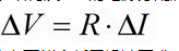
The entire power supply system must ensure that each integrated circuit device is provided with a stable voltage within the normal range. However, switching currents and parasitic high-frequency effects in the power supply system always introduce voltage noise. Its voltage change can be calculated by the following formula:
Here ΔV is the voltage fluctuation observed at the device, and ΔI is the switching current. Z is the input impedance between the power supply and ground of the entire power supply system observed at the device. In order to reduce voltage fluctuations, the power supply and ground should be kept low. In the DC case, since Z becomes a pure resistor, low resistance corresponds to a low power supply IR drop. In the AC case, low resistance can also reduce the transient noise generated by the switching current. Of course, this requires Z to be kept small over a wide frequency band.
Note that the power supply and ground are usually used as signal loops and reference planes, so there is a close relationship between the power supply system and the signal distribution system.
However, due to space limitations, the noise phenomenon of the power supply system introduced by synchronous switching noise (IO SSO) and the current loop control problem will not be discussed here. The following sections will ignore the signal system and focus solely on the analysis of the power supply system.
DC IR Drop
Since the characteristic size of the chip’s power grid is very small (a few microns or even smaller), the resistance loss in the chip is serious, so the IR drop in the chip has been widely studied. In the following cases, the IR drop on the PCB (in the range of tens to hundreds of millivolts) will also have a greater impact on high-speed system design.
The power board layer has Swiss-Chess structure, Neck-Down structure and the board plane is divided due to dynamic routing (Figure 1); the number of device pins, vias, solder balls, C4 bumps through which the current passes on the power board layer is insufficient, the thickness of the power board is insufficient, and the current path is unbalanced; the system design requires low voltage, high current, and a tight voltage floating range.

Figure 1: Some common physical structure designs on PCB that increase the resistance of the current path
For example, a high-density and high-pin device often forms the so-called Swiss-Chess structure effect on the chip packaging structure and the power distribution layer of the PCB due to a large number of vias and anti-pads. The Swiss-Chess structure will produce many small metal areas with high resistance. According to
Due to such a high-resistance current path in the power supply system, the voltage or current sent to the components on the PCB may be lower than the design requirements. Therefore, a good DC IR voltage drop simulation is the key to estimating the allowable voltage drop range of the power supply system. Through various possible analyses, design solutions or rules are provided before and after layout and routing.
Layout engineers, system engineers, signal integrity engineers and power design engineers can also combine IR drop analysis in the constraint manager as a final verification tool (DRC) for design rule verification of each power and ground net list on the PCB. This design process through automated software analysis can avoid layout and wiring problems on the complex power supply system structure that cannot be discovered by visual inspection or even experience. Figure 2 shows that IR drop analysis can accurately point out the distribution of key voltage and current in the power supply system on a high-performance PCB.
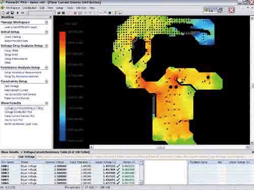
Figure 2: Sigrity PowerDC calculates the current distribution on the power board layer
AC power ground impedance analysis
Many people know that a pair of metal plates form a flat plate capacitor, so they think that the characteristic of the power board layer is to provide a flat plate capacitor to ensure the stability of the power supply voltage. At low frequencies, when the signal wavelength is much larger than the size of the plate, the power board layer and the ground do form a capacitor.
However, when the frequency increases, the characteristics of the power board layer begin to become complicated. More precisely, a pair of plates form a flat transmission line system. The noise between the power supply and the ground, or the corresponding electromagnetic field, propagates between the plates according to the transmission line principle. When the noise signal propagates to the edge of the plate, part of the high-frequency energy will radiate out, but a larger part of the energy will be reflected back. Multiple reflections from different boundaries of the plate constitute the resonance phenomenon in the PCB.
In AC analysis, the power ground impedance resonance of the PCB is a unique phenomenon. Figure 3 shows the input impedance of a pair of power board layers. For comparison, the impedance characteristics of a pure capacitor and a pure inductor are also drawn in the figure. The size of the board is 30cm×20cm, the spacing between the boards is 100um, and the filling medium is FR4 material. The power rectifier module on the board is replaced by a 3nH inductor. The capacitor showing the pure capacitive impedance characteristic is a 20nF capacitor. It can be seen from the figure that when there is no power rectifier module on the board, the impedance characteristics of the plate (red line) and the capacitor (blue line) are the same in the frequency range of tens of megahertz. Above 100MHz, the impedance characteristics of the plate are inductive (along the green line). After reaching the frequency range of hundreds of megahertz, the appearance of several resonance peaks shows the resonance characteristics of the plate, and the plate is no longer purely inductive.
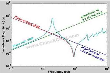
Figure 3: Input impedance of the board pair with and without the power rectifier module
At this point, it is clear that a low-impedance power supply system (from DC to AC) is the key to obtaining low voltage fluctuations: reducing the inductance, increasing the capacitance, and eliminating or reducing those resonant peaks are the design goals.
In order to reduce the impedance of the power supply system, some design guidelines should be followed:
- Reduce the spacing between the power supply and the floor layer;
- Increase the size of the board;
- Increase the dielectric constant of the filling medium;
- Use multiple pairs of power and floor layers.
However, due to manufacturing or some other design considerations, design engineers also need to use some more flexible and effective methods to change the impedance of the power supply system. In order to reduce the impedance and eliminate those resonant peaks, placing discrete decoupling capacitors on the PCB has become a common method.
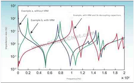
Figure 4 shows the input impedance of the power supply system calculated by Sigrity PowerSI under three different settings:
Figure 4: PCB input impedance curve calculated by PowerSI under three settings. (a) does not include the power rectifier module; (b) includes the power rectifier module; (c) includes the power rectifier module and some decoupling capacitors
a. There is no power rectifier module and no decoupling capacitors are placed on the board.
b. The power rectifier module is simulated by a short circuit and no decoupling capacitors are placed on the board.
c. The power rectifier module is simulated by a short circuit and the decoupling capacitors are placed on the board.
As can be seen from the figure, the blue line of example a, the input impedance of the power supply system observed at the location of the integrated circuit chip is capacitive at low frequencies. As the frequency increases, the first natural resonance peak appears at a frequency of 800MHz. The wavelength of this frequency corresponds to the size of the power ground plate.
The green line of example b, the input impedance is inductive at low frequencies. This corresponds exactly to the loop inductance from the location of the integrated circuit chip to the power rectifier module. This loop inductance and the plate capacitor together introduce a resonance peak at 200MHz.
In the red line of example c, after placing some decoupling capacitors on the board, the 200MHz resonance peak is moved to a very low frequency (<20MHz), and the peak value of the resonance peak is also reduced a lot. The first strong resonance peak appears at about 1GHz. It can be seen that by placing discrete decoupling capacitors on the PCB, the power supply system can achieve a lower and smoother AC impedance response in the main operating frequency range. Therefore, the noise of the power supply system will also be very low.
Placing discrete decoupling capacitors on the board allows designers to flexibly adjust the impedance of the power supply system and achieve lower power ground noise. However, how to choose the placement, how many and what kind of decoupling capacitors to choose is still a series of design issues. Therefore, it is often necessary to find the best decoupling solution for a specific design, use appropriate design software, and perform a lot of power supply system simulations.
Co-design concept
Figure 4 actually reveals another very important fact, that is, the frequency range of discrete decoupling capacitors placed on the PCB can only reach a few hundred megahertz. At higher frequencies, the parasitic inductance of each discrete decoupling capacitor and the loop inductance of the board layer and via (capacitor to chip) will greatly reduce the decoupling effect. It is not possible to further reduce the input impedance of the power supply system by simply placing discrete decoupling capacitors on the PCB. From a few hundred megahertz to higher frequencies, the inter-board capacitance of the power supply system of the package structure and the discrete decoupling capacitors placed on the package structure will start to play a role. In the GHz frequency range, the capacitance between the power grids in the chip and the decoupling capacitors in the chip are the only decoupling solutions.
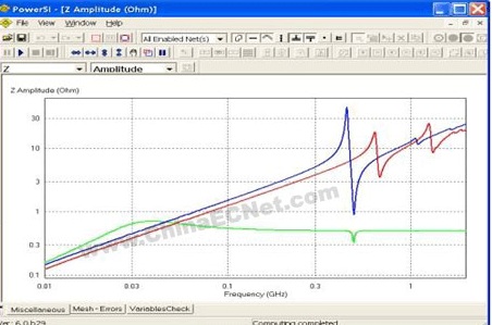
Figure 5 shows an example. The red line is the input impedance obtained after placing some discrete decoupling capacitors on the PCB.
The first resonance peak appears at 600MHz to 700MHz. After considering the package structure, the additional package inductance shifts the resonance peak to about 450MHz, see the blue line. After including the chip power supply system, the decoupling capacitors in the chip remove all those high-frequency resonance peaks, but at the same time introduce a very weak 30MHz resonance peak, see the green line. This 30MHz resonance will be reflected in the time domain as a voltage trough on the intermediate frequency envelope of the high-frequency flip signal.
Figure 5: Input impedance calculated for different structures. Without considering the chip and package structure (red line); considering the package structure (blue line); considering the chip, package and circuit board (green line)
Decoupling within the chip is very effective, but the cost is to use up valuable space within the chip and consume more leakage current. Moving the decoupling capacitors within the chip to the package structure may be a good compromise, but it requires designers to have knowledge of the entire system from chip, package structure to PCB. But usually, PCB designers cannot obtain the design data of the chip and package structure and the corresponding simulation software package. For integrated circuit designers, they usually do not care about the design of the lower-end package and circuit board. But it is obvious that the use of collaborative design concepts to optimize the analysis and design of the power supply system of the entire system, chip-package-circuit board is a future development trend. Some companies at the forefront of electronic design have actually done so.


