Andwin PCB SMT
In the modern electronics manufacturing industry,surface mount technology(SMT)has become a core process for circuit board assembly,driving the miniaturization and high density advancement of electronic devices.Andwin PCB,a key player in the industry,stands out in the fiercely competitive market thanks to its sophisticated SMT process technology.
In the modern electronics manufacturing industry,surface mount technology(SMT)has become a core process for circuit board assembly,replacing traditional manual insertion methods and driving the miniaturization and high-density advancement of electronic devices.
As a core process in electronics manufacturing, SMT occupies a vital position in the electronics industry chain in Hefei. This article will provide an in-depth understanding of Anda PCB’s SMT technology and explore how it has become a core driving force in electronics manufacturing.
Introduction to SMT Technology
Surface mount technology (SMT) is a next-generation electronics assembly technology developed from hybrid integrated circuit technology. Characterized by the use of surface mounting components and reflow soldering, it has become a new generation of assembly technology in electronic product manufacturing. The application of SMT has promoted the miniaturization and multifunctionality of electronic products, facilitating high-volume production with low defect rates.
The basic SMT process consists of screen printing (or dispensing), placement (curing), reflow soldering, cleaning, testing, and rework. This meticulously coordinated, integrated process forms the foundation for the miniaturization and high performance of modern electronic devices.
Andwin PCB’s Core SMT Process
1.Production Preparation
The starting point of SMT is the standardization of the environment and materials. Anda PCB’s workshop maintains a constant temperature and humidity (25±3°C, 45%-70% humidity), is equipped with an electrostatic protection system, and strictly controls light intensity to 1000±200 lux.
Material management is paramount. Solder paste follows the “first-in, first-out” principle and must be warmed and stirred for four hours before opening to prevent post-solder scattering caused by low temperatures. Stencils are typically 0.12-0.15mm thick, with openings 4μm smaller than the PCB pads to prevent solder paste collapse and short circuits. Sensitive components (such as IC chips) must be stored in a moisture-proof manner. Humidity test kits are invalidated when they turn pink to prevent oxidation-induced solder joints.
2.Solder Paste Printing Technology
Solder paste printing is the first core step in the SMT placement process, and its quality directly impacts the reliability of subsequent placement and soldering. Anda PCB uses stencils to precisely transfer solder paste to PCB pads, maintaining uniformity and thickness tolerances within ±15%.
Printing precision control focuses on stencil aperture design, typically requiring the opening size to match the pad within ±5%. Squeegee pressure is also adjusted based on PCB thickness variations (recommended range: 4-8 kg/cm²). Printing speeds must be maintained within a dynamic range of 30-150mm/s. Faster speeds can easily lead to insufficient solder paste filling, while slower speeds can cause collapse defects.
For fine-pitch components (such as the 0201 package), Anda PCB uses nano-coated steel meshes to reduce demolding resistance and an optical alignment system to control printing offset within ±25μm. The placement process must be completed within 2 hours after printing to prevent excessive evaporation of solder paste solvents that could affect soldering activity.
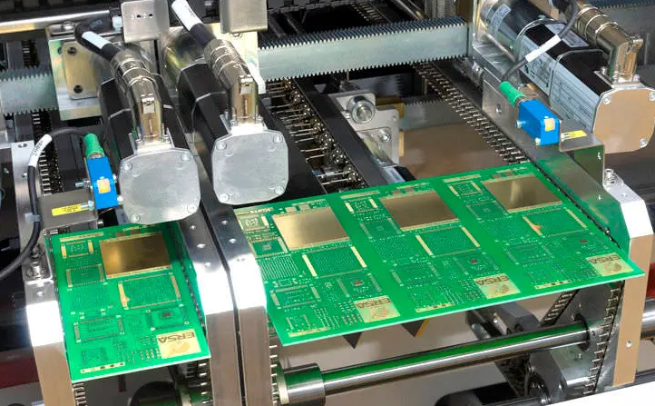
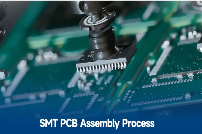
3.Precision Component Placement
The placement process involves accurately attaching surface mount components to fixed locations on the PCB. Anda PCB utilizes high-precision placement machines that utilize a vacuum nozzle and vision positioning system to achieve stable placement of 01005 micro-components and BGA packaged devices.
During equipment operation, it is crucial to control the Z-axis pressure (typically set within the 3-5N range) and placement speed (CPH ≥ 35,000). For 0.4mm pitch QFP chips, Anda PCB uses dual-camera vision alignment technology with an optical resolution of 5μm, accurately identifying positional deviations between pads and pins.
Practical experience shows that when placement offset is controlled within 15% of the component size, the risk of short circuits after reflow soldering can be reduced by 72%. Operators regularly check nozzle vacuum (standard value ≥ -85kPa) and establish a component polarity database to avoid process defects such as reverse placement.
4.Reflow Soldering Process
Reflow soldering remelts pre-dispensed solder paste onto the printed circuit board pads to achieve mechanical and electrical connections between the terminals or pins of surface mount components and the printed circuit board pads.
Anda PCB precisely controls the temperature gradient to ensure a reliable metallurgical bond between the solder paste and the solder. The reflow soldering process is divided into four stages:
Preheating zone (1-2°C/second to 150°C): Solvent evaporation to prevent solder spatter;
Soaking zone (60-90 seconds to 183°C): Activate flux and remove oxides;
Reflow zone (peak temperature 215±10°C, 45-60 seconds): Complete solder paste melting;
Cooling zone (slope 2-4°C/second): Alloy solder joints solidify.
A 5°C deviation in peak temperature can cause BGA ball weld defects. Therefore, Anda PCB uses an oven temperature tester for calibration every 12 hours or during line changes. For high-density PCBs or BGA packaged components, the reflow zone peak temperature is typically set at 230-250°C, with a duration strictly limited to 20-40 seconds to prevent pad oxidation and component thermal damage.
5.Quality Inspection and Control
Quality inspection is a critical step in ensuring product reliability. Anda PCB has established a multi-level quality verification system:
AOI (Automated Optical Inspection): Through high-precision image acquisition and algorithm analysis, the system monitors the quality of solder paste printing, component placement, and post-soldering in real time. Based on IPC-A-610H specifications, the inspection system establishes tiered criteria for typical defects such as component offset, reversed polarity, and insufficient solder paste coverage.
X-Ray Inspection: For hidden solder joints such as BGAs and CSPs, Anda PCB utilizes 180kV high-voltage microfocus X-ray equipment, coupled with digital image processing algorithms, to achieve ±5μm-level solder joint morphology analysis. X-rays can penetrate multi-layer PCB structures and accurately identify the bottom solder joints of packaged components like BGAs and QFNs, achieving a detection rate exceeding 98% for typical defects such as cold solder joints, bridging, and air voids.
SPC (Statistical Process Control): By collecting real-time production data and linking it to the MES system, Anda PCB has significantly improved its process anomaly warning and traceability capabilities, laying the foundation for the complex requirements of subsequent BGA/CSP packaging processes.
Advantages and Applications of SMT Technology
SMT technology offers significant advantages: high assembly density, compact size, and light weight; high reliability, strong vibration resistance, and low solder joint defect rates; excellent high-frequency characteristics, reducing electromagnetic and radio frequency interference; and ease of automation, improving production efficiency.
These advantages have led to its widespread application in PCs and peripherals, automotive electronics, medical equipment, communications products, consumer electronics, and other fields.
In particular, in the automotive electronics sector, the development of automotive control systems, such as instrument panel displays, air quality, audio, displays, and sensors, requires high signal transmission and reliability, making flexible printed circuits (FPCs) increasingly advantageous.
Future Development Direction of Anda PCB
With the continuous advancement of informatization and intelligentization, market demand for PCBs and SMT technology is also increasing. Anda PCB is actively planning future technological development directions:
High Speed and High Precision: SMT machines have achieved breakthroughs in accuracy of ±0.001mm, supporting ultra-micro components as small as 01005. Production lines are becoming more integrated, and dual-track reflow soldering enables two lines to share equipment, saving 30% space.
Green Smart Manufacturing: Lead-free soldering is now widely adopted, and AI algorithms optimize furnace temperature profiles in real time. IoT platforms monitor equipment status and enable predictive maintenance to reduce downtime.
Flexible Production: Modular placement machines enable rapid line switching, and 3D-printed stencils enable same-day delivery of customized circuit boards.
Conclusion
Precise collaboration throughout the entire SMT process has established the foundation for the miniaturization and high performance of modern electronic devices. From micron-level control of solder paste printing to temperature control during reflow soldering, to AI-driven visual inspection, stringent standards at every stage contribute to the quality of electronics manufacturing.
Anda PCB continuously improves the precise coordination of the SMT process chain and the dynamic control of process parameters. This not only ensures uniform solder paste printing, stable debugging of high-precision placement equipment, and scientific optimization of reflow soldering profiles, but also lays a solid foundation for the quality of modern electronic assembly.
With domestic high-speed placement machines exceeding ±0.001mm accuracy, 3D-printed stencils achieving same-day delivery, and the widespread use of AI for real-time yield optimization, SMT technology is evolving from “precision manufacturing” to “zero-defect intelligent manufacturing.” This process will not only drive the continuous evolution of products such as mobile phones and new energy vehicles, but will also reshape the global electronics industry chain.


