Anti-interference design of RF circuit board
Abstract: In order to ensure the circuit performance, electromagnetic compatibility should be considered when designing the RF circuit printed circuit board (PCB), which is of great significance for reducing the electromagnetic information radiation of the system. This paper focuses on the layout and wiring principles of components to maximize the performance indicators of the circuit and achieve the design purpose of anti-interference. Through several experimental test cases, several different factors affecting the anti-interference performance of the printed circuit board are analyzed, and the practical solutions that should be taken in the production process of the printed circuit board are explained.
Introduction
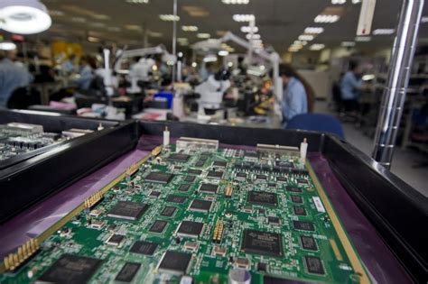
With the development of communication technology, wireless RF circuit technology is more and more widely used. The performance indicators of the RF circuit directly affect the quality of the entire product. The anti-interference design of the RF circuit printed circuit board (PCB) is of great significance for reducing the electromagnetic information radiation of the system. The density of RF circuit PCB is getting higher and higher.
The quality of PCB design has a great influence on the anti-interference ability. The same circuit, different PCB design structures, and their performance indicators will vary greatly. If the electromagnetic interference signal is not handled properly, it may cause the entire circuit system to fail to work properly.
Therefore, how to prevent and suppress electromagnetic interference and improve electromagnetic compatibility has become a very important topic in the design of RF circuit PCB.
Electromagnetic compatibility (EMC) refers to the ability of an electronic system to work normally in a specified electromagnetic environment according to the design requirements. The electromagnetic interference to the electronic system comes not only from the radiation of the electric field and magnetic field, but also from the influence of the line common impedance, the coupling between the wires and the circuit structure. When developing and designing circuits, it is hoped that the designed printed circuit board is as unaffected by external interference as possible, and also interferes with other electronic systems as little as possible.
The first task of designing a printed circuit board is to analyze the circuit and determine the key circuit.
This is to identify which circuits are interference sources and which circuits are sensitive circuits, and to find out through what paths the interference source may interfere with the sensitive circuit. The operating frequency of the RF circuit is high, and the interference source mainly interferes with the sensitive circuit through electromagnetic radiation. Therefore, the purpose of the anti-interference design of the RF circuit PCB board is to reduce the electromagnetic radiation of the PCB board and the crosstalk between the circuits on the PCB board.
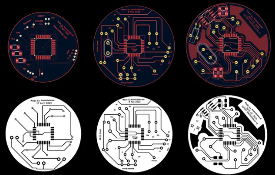
1 RF circuit board design
- 1 Component layout
Since SMT generally uses infrared furnace hot flow soldering to achieve component soldering, the layout of components affects the quality of the solder joints, and thus affects the product yield. As for the RF circuit PCB design, electromagnetic compatibility requires that each circuit module should not generate electromagnetic radiation as much as possible and have a certain anti-electromagnetic interference ability.
Therefore, the layout of components also affects the interference and anti-interference ability of the circuit itself, which is directly related to the performance of the designed circuit. Therefore, in addition to considering the layout of ordinary PCB design when designing RF circuit PCB, it is also necessary to consider how to reduce the mutual interference between the various parts of the RF circuit, how to reduce the interference of the circuit itself to other circuits, and the anti-interference ability of the circuit itself.
According to experience, the effect of the RF circuit depends not only on the performance indicators of the RF circuit board itself, but also largely on the mutual influence with the CPU processing board. Therefore, when designing PCB, reasonable layout is particularly important.
The general principle of layout is that components should be arranged in the same direction as much as possible, and the phenomenon of poor welding can be reduced or even avoided by selecting the direction in which the PCB enters the tin melting system;
according to experience, there should be at least 0.5mm spacing between components to meet the tin melting requirements of components. If the space of the PCB board allows, the spacing between components should be as wide as possible. For double-sided boards, one side should generally be designed with SMD and SMC components, and the other side should be discrete components.
The layout should pay attention to:
1) First determine the position of the interface components with other PCB boards or systems on the PCB board, and pay attention to the coordination between the interface components (adding the direction of the components, etc.);
2) Because the volume of handheld products is very small, the components are arranged very compactly, so for the components with larger volume, priority must be given to determine the corresponding position, and consider the coordination between them;
3) Carefully analyze the circuit structure, divide the circuit into blocks (add high-frequency amplification circuit, mixing circuit and demodulation circuit, etc.), separate the strong electric signal and the weak electric signal as much as possible, separate the digital signal circuit and the analog signal circuit, and arrange the circuits that complete the same function within a certain range as much as possible to reduce the signal loop area; the filter network of each part of the circuit must be connected nearby, which can not only reduce radiation, but also reduce the probability of interference and improve the anti-interference ability of the circuit;
4) Group the unit circuits according to their different sensitivity to electromagnetic compatibility during use. When laying out the components that are susceptible to interference in the circuit, interference sources (such as interference from the CPU on the data processing board, etc.) should be avoided as much as possible.
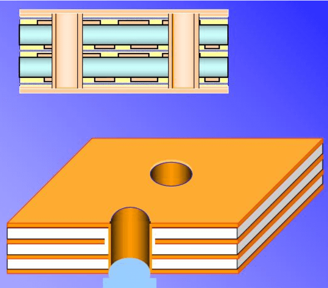
- 2 Wiring
After the layout of the components is basically completed, wiring can be started. The basic principle of wiring is: when the assembly density permits, try to use low-density wiring design, and the signal routing should be as consistent as possible to facilitate impedance matching.
For RF circuits, unreasonable design of the direction, width, and line spacing of signal lines may cause cross interference between signal transmission lines; in addition, the system power supply itself also has noise interference, so when designing the time-frequency circuit PCB, comprehensive consideration must be given to reasonable wiring. When wiring, all routing lines should be about 2 mm away from the border of the PCB board to avoid the risk of disconnection or disconnection during PCB board production.
The power line should be as wide as possible to reduce loop resistance. At the same time, the direction of the power line and ground line should be consistent with the direction of data transmission to improve anti-interference ability. The signal line should be as short as possible and the number of vias should be minimized. The connection between components should be as short as possible to reduce distributed parameters and mutual electromagnetic interference. Incompatible signal lines should be kept as far away from each other as possible, and parallel routing should be avoided as much as possible. The signal lines on the front and back sides should be perpendicular to each other. When wiring, 135° should be used where corners are required.