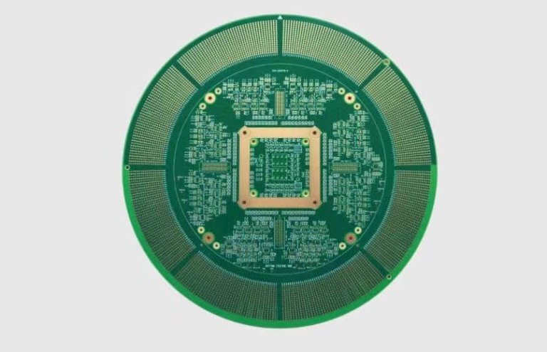
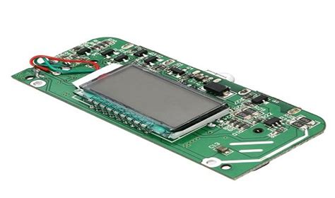
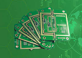
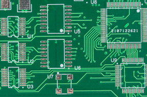
Aoi in pcb manufacturing
Automated Optical Inspection: Enhancing PCB Quality Control
Automated Optical Inspection (AOI) has become an indispensable tool in the realm of Printed Circuit Board (PCB) manufacturing, significantly enhancing the quality control process. As the demand for more complex and miniaturized electronic devices continues to grow, the need for precise and reliable inspection methods has never been more critical.
AOI systems, leveraging advanced imaging technologies and sophisticated algorithms, offer a robust solution to the challenges faced in ensuring the integrity and functionality of PCBs.
To begin with, AOI systems utilize high-resolution cameras to capture detailed images of PCBs at various stages of the manufacturing process.
These images are then analyzed using powerful software that can detect a wide range of defects, including soldering issues, component misalignments, and surface irregularities. By comparing the captured images to a predefined set of standards or a golden sample, AOI systems can quickly and accurately identify deviations that may compromise the performance of the final product. This capability is particularly valuable in high-volume production environments, where manual inspection would be both time-consuming and prone to human error.
Moreover, the integration of AOI into the PCB manufacturing workflow offers several key advantages.
One of the most significant benefits is the ability to perform real-time inspections, allowing for immediate feedback and corrective actions. This not only helps in maintaining consistent quality but also reduces the likelihood of defective products reaching the end customer. Additionally, AOI systems can be programmed to inspect specific areas of interest, such as critical solder joints or high-density component placements, ensuring that even the most challenging aspects of PCB assembly are thoroughly examined.
Another noteworthy aspect of AOI is its role in process optimization.
By collecting and analyzing inspection data, manufacturers can gain valuable insights into the root causes of defects and implement targeted improvements. For instance, if a particular type of defect is consistently detected in a specific area of the PCB, it may indicate an issue with the soldering process or the placement accuracy of certain components. Addressing these issues at their source can lead to significant enhancements in overall production efficiency and product reliability.
Furthermore, the adoption of AOI technology aligns with the broader trend towards Industry 4.0 and the smart factory paradigm.
As manufacturing processes become increasingly automated and interconnected, the ability to seamlessly integrate AOI systems with other production equipment and data management platforms becomes crucial. This integration enables a more holistic approach to quality control, where inspection results can be correlated with other process parameters to provide a comprehensive view of the manufacturing environment. Consequently, manufacturers can achieve higher levels of precision and consistency, ultimately leading to better product quality and customer satisfaction.
In addition to its technical benefits, AOI also offers economic advantages.
By reducing the incidence of defects and rework, manufacturers can lower their production costs and improve their bottom line. The initial investment in AOI technology is often offset by the savings realized through increased yield and reduced waste. Moreover, the ability to deliver high-quality products consistently can enhance a company’s reputation and competitiveness in the market.
In conclusion, Automated Optical Inspection represents a significant advancement in PCB manufacturing, providing a powerful means of enhancing quality control. Through its ability to perform precise, real-time inspections and facilitate process optimization, AOI plays a crucial role in ensuring the reliability and performance of modern electronic devices. As the industry continues to evolve, the integration of AOI technology will undoubtedly remain a key factor in achieving excellence in PCB production.
The Role Of AOI In Reducing PCB Manufacturing Defects
In the intricate world of printed circuit board (PCB) manufacturing, ensuring the highest quality and reliability is paramount. One of the most effective tools in achieving this goal is Automated Optical Inspection (AOI).
AOI plays a crucial role in reducing defects during the PCB manufacturing process, thereby enhancing the overall quality and performance of the final product. By leveraging advanced imaging and processing technologies, AOI systems meticulously inspect PCBs for a wide range of potential defects, ensuring that only the highest quality boards make it through to the next stages of production.
To begin with, AOI systems utilize high-resolution cameras and sophisticated algorithms to capture and analyze images of PCBs.
This process allows for the detection of various defects, such as soldering issues, component misalignments, and surface irregularities. By identifying these defects early in the manufacturing process, AOI helps to prevent faulty boards from progressing further down the production line, thereby reducing the likelihood of costly rework or scrapping.
Moreover, the ability to detect defects at an early stage ensures that corrective actions can be taken promptly, minimizing the impact on production schedules and overall costs.
Furthermore, the implementation of AOI in PCB manufacturing significantly enhances the consistency and reliability of inspections.
Unlike manual inspection methods, which are prone to human error and fatigue, AOI systems provide a high level of accuracy and repeatability. This consistency is particularly important in high-volume production environments, where even minor defects can lead to significant issues if left undetected. By automating the inspection process, AOI ensures that each PCB is subjected to the same rigorous scrutiny, thereby maintaining a consistently high standard of quality across all boards.
In addition to improving defect detection, AOI also contributes to the optimization of the manufacturing process.
The data collected by AOI systems can be analyzed to identify trends and patterns in defect occurrences, providing valuable insights into potential areas for process improvement. For instance, if a particular type of defect is consistently detected in a specific area of the PCB, this information can be used to pinpoint the root cause and implement corrective measures.
Consequently, AOI not only helps to reduce the incidence of defects but also drives continuous improvement in the manufacturing process, leading to greater efficiency and productivity.
Moreover, the integration of AOI with other advanced manufacturing technologies, such as surface mount technology (SMT) and in-circuit testing (ICT), further enhances its effectiveness in reducing PCB defects.
By combining the strengths of these complementary technologies, manufacturers can achieve a more comprehensive and robust inspection process.
For example, while AOI excels at detecting visual defects, ICT can identify electrical issues that may not be visible to the naked eye. Together, these technologies provide a holistic approach to quality assurance, ensuring that PCBs meet the highest standards of performance and reliability.
In conclusion, the role of AOI in reducing PCB manufacturing defects cannot be overstated. By providing accurate, consistent, and comprehensive inspections, AOI helps to ensure that only the highest quality boards make it through to the final stages of production. Additionally, the insights gained from AOI data enable manufacturers to continuously improve their processes, further enhancing the quality and efficiency of PCB manufacturing. As the demand for high-performance electronic devices continues to grow, the importance of AOI in maintaining the integrity and reliability of PCBs will only become more pronounced.
Integrating AOI Systems In Modern PCB Production Lines
In the ever-evolving landscape of electronics manufacturing, the integration of Automated Optical Inspection (AOI) systems into modern Printed Circuit Board (PCB) production lines has become a pivotal advancement.
As the demand for smaller, more complex, and highly reliable electronic devices continues to surge, manufacturers are compelled to adopt innovative technologies that enhance both efficiency and quality. AOI systems, with their ability to meticulously inspect PCBs for defects, have emerged as indispensable tools in this quest for excellence.
To begin with, the primary function of AOI systems in PCB manufacturing is to ensure that each board meets stringent quality standards.
These systems employ high-resolution cameras and sophisticated algorithms to capture and analyze images of the PCB at various stages of production. By comparing these images to predefined standards, AOI systems can detect a wide array of defects, including misaligned components, soldering issues, and surface irregularities. This automated inspection process not only accelerates the identification of defects but also significantly reduces the likelihood of human error, which can be prevalent in manual inspection methods.
Moreover, the integration of AOI systems into PCB production lines offers substantial benefits in terms of process optimization.
By providing real-time feedback on the quality of the boards, AOI systems enable manufacturers to promptly address any issues that arise during production. This immediate feedback loop facilitates continuous improvement, as manufacturers can quickly implement corrective actions to mitigate defects and enhance overall product quality. Consequently, this leads to a reduction in rework and scrap rates, ultimately resulting in cost savings and increased production efficiency.
In addition to process optimization, AOI systems play a crucial role in ensuring compliance with industry standards and regulations.
As electronic devices become more ubiquitous and integral to various applications, the need for reliable and safe products has never been greater. AOI systems help manufacturers adhere to rigorous quality control standards, such as IPC-A-610, which governs the acceptability of electronic assemblies. By ensuring that each PCB meets these standards, AOI systems contribute to the production of high-quality, reliable electronic devices that meet the expectations of both consumers and regulatory bodies.
Furthermore, the integration of AOI systems into PCB production lines is not without its challenges.
One of the primary considerations is the initial investment required for the acquisition and implementation of these systems. While the cost can be significant, it is important to recognize that the long-term benefits, including improved quality, reduced rework, and enhanced efficiency, often outweigh the initial expenditure. Additionally, manufacturers must ensure that their workforce is adequately trained to operate and maintain AOI systems. This may involve investing in training programs and ongoing education to keep pace with technological advancements.
Despite these challenges, the advantages of integrating AOI systems into modern PCB production lines are undeniable.
As the electronics industry continues to advance, the need for precise, efficient, and reliable inspection methods will only grow. AOI systems, with their ability to deliver consistent and accurate results, are well-positioned to meet this demand. By embracing these systems, manufacturers can not only enhance the quality of their products but also gain a competitive edge in an increasingly demanding market.
In conclusion, the integration of AOI systems into modern PCB production lines represents a significant step forward in the pursuit of manufacturing excellence. Through their ability to detect defects, optimize processes, and ensure compliance with industry standards, AOI systems have become essential tools for manufacturers striving to meet the ever-growing demands of the electronics market. While the initial investment and training requirements may pose challenges, the long-term benefits of improved quality, efficiency, and cost savings make AOI systems a worthwhile addition to any PCB production line.
Cost-Benefit Analysis Of Implementing AOI In PCB Manufacturing
Automated Optical Inspection (AOI) has become an integral part of the printed circuit board (PCB) manufacturing process, offering a blend of precision and efficiency that manual inspection methods simply cannot match. As the electronics industry continues to evolve, the cost-benefit analysis of implementing AOI in PCB manufacturing becomes increasingly relevant. This analysis is crucial for manufacturers aiming to balance quality control with cost-effectiveness.
To begin with, the initial investment in AOI systems can be substantial. High-quality AOI machines, equipped with advanced imaging and processing capabilities, often come with a hefty price tag.
Additionally, there are costs associated with training personnel to operate these sophisticated systems. However, these upfront expenses should be viewed in the context of long-term gains. One of the most significant benefits of AOI is its ability to detect defects early in the production process. By identifying issues such as misaligned components, soldering defects, and other anomalies at an early stage, AOI helps prevent defective products from progressing further down the production line. This early detection not only reduces the cost of rework and scrap but also minimizes the risk of defective products reaching the customer, thereby protecting the manufacturer’s reputation.
Moreover, AOI systems offer unparalleled speed and accuracy compared to manual inspection.
Human inspectors, no matter how skilled, are prone to fatigue and errors, especially when dealing with high-volume production runs. In contrast, AOI systems can operate continuously with consistent accuracy, ensuring that every PCB is inspected to the same high standard. This consistency is particularly important in industries where reliability and performance are critical, such as aerospace, medical devices, and automotive electronics. By maintaining a high level of quality control, manufacturers can meet stringent industry standards and regulatory requirements, which can open up new market opportunities and drive business growth.
Another important aspect to consider is the data-driven insights provided by AOI systems.
These machines not only identify defects but also collect valuable data on the types and frequencies of defects occurring in the production process. This data can be analyzed to identify trends and root causes, enabling manufacturers to implement targeted improvements in their processes. For instance, if a particular type of defect is consistently detected, it may indicate an issue with a specific component or a step in the manufacturing process. By addressing these issues proactively, manufacturers can enhance overall process efficiency and product quality, leading to cost savings in the long run.
Furthermore, the integration of AOI with other automated systems in a smart manufacturing environment can lead to even greater efficiencies. For example, AOI data can be fed into a Manufacturing Execution System (MES) to provide real-time feedback and enable dynamic adjustments to the production process. This level of integration supports a more agile and responsive manufacturing operation, capable of adapting to changes in demand and production requirements with minimal disruption.
In conclusion, while the initial costs of implementing AOI in PCB manufacturing can be significant, the long-term benefits far outweigh these expenses. The ability to detect defects early, maintain consistent quality, gain valuable process insights, and integrate with other automated systems makes AOI a worthwhile investment. For manufacturers committed to delivering high-quality products and staying competitive in a rapidly evolving industry, the adoption of AOI is not just a cost but a strategic advantage.
Future Trends In AOI Technology For PCB Manufacturing
Automated Optical Inspection (AOI) technology has become an indispensable tool in the realm of Printed Circuit Board (PCB) manufacturing, ensuring high-quality standards and minimizing defects.
As the electronics industry continues to evolve, the future of AOI technology is poised for significant advancements, driven by the increasing complexity of PCBs and the demand for higher precision and efficiency. One of the most notable trends in AOI technology is the integration of artificial intelligence (AI) and machine learning algorithms.
These technologies enable AOI systems to learn from past inspections, improving their accuracy and reducing false positives over time. By analyzing vast amounts of data, AI-driven AOI systems can identify patterns and anomalies that might be missed by traditional inspection methods.
This not only enhances the reliability of the inspection process but also allows for predictive maintenance, where potential issues can be identified and addressed before they lead to costly production downtimes.
In addition to AI, the incorporation of advanced imaging tecnologies is set to revolutionize AOI systems.
High-resolution cameras and 3D imaging techniques provide a more detailed and accurate representation of the PCB, allowing for the detection of even the smallest defects. These imaging advancements are particularly crucial as PCBs become more intricate, with smaller components and tighter tolerances. The ability to inspect these complex boards with greater precision ensures that manufacturers can maintain the highest quality standards while meeting the demands of modern electronics.
Another emerging trend in AOI technology is the shift towards inline inspection systems.
Unlike traditional AOI systems, which are typically used at the end of the production line, inline AOI systems are integrated directly into the manufacturing process. This allows for real-time inspection and immediate feedback, enabling manufacturers to identify and correct defects as they occur.
The result is a more efficient production process with reduced waste and higher yields. Furthermore, inline AOI systems can be seamlessly integrated with other manufacturing equipment, creating a more cohesive and automated production environment.
The rise of Industry 4.0 and the Internet of Things (IoT) is also influencing the future of AOI technology. By connecting AOI systems to a network of smart devices and sensors, manufacturers can gain deeper insights into their production processes. This connectivity allows for the collection and analysis of data from multiple sources, providing a comprehensive view of the manufacturing environment. With this information, manufacturers can optimize their processes, improve quality control, and make more informed decisions. Additionally, the ability to remotely monitor and control AOI systems through IoT connectivity offers greater flexibility and convenience, particularly for large-scale manufacturing operations.
As environmental concerns continue to grow, the future of AOI technology will also be shaped by the need for sustainable manufacturing practices. Energy-efficient AOI systems, coupled with the use of eco-friendly materials and processes, will become increasingly important. Manufacturers will need to balance the demands for high-quality PCBs with the need to minimize their environmental impact. By adopting sustainable AOI technologies, manufacturers can reduce their carbon footprint and contribute to a more sustainable future.
In conclusion, the future of AOI technology in PCB manufacturing is set to be defined by advancements in AI, imaging technologies, inline inspection systems, and IoT connectivity. These innovations will not only enhance the accuracy and efficiency of the inspection process but also enable manufacturers to meet the growing demands of the electronics industry while maintaining high-quality standards. As the industry continues to evolve, embracing these trends will be crucial for manufacturers looking to stay competitive and achieve long-term success.