Application of flexible pcb
Introduction To Printed Circuit Boards: Understanding The Basics
Printed Circuit Boards (PCBs) are fundamental components in modern electronic devices, serving as the backbone that supports and connects various electronic components. To understand the basics of PCBs, it is essential to explore their structure, function, and significance in the electronics industry.
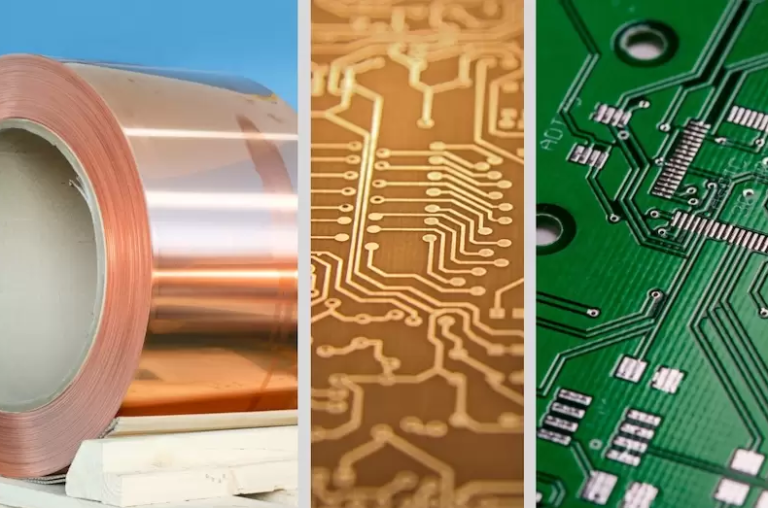
At the core, a PCB is a flat board made from non-conductive material, typically fiberglass, which provides a sturdy base for mounting electronic components.
These components are interconnected through conductive pathways, or traces, which are etched onto the board’s surface using copper. This intricate network of traces allows for the efficient transmission of electrical signals between components, enabling the device to function as intended.
The evolution of PCBs has been pivotal in the miniaturization and advancement of electronic devices.
Before the advent of PCBs, electronic circuits were constructed using point-to-point wiring, a labor-intensive and error-prone process. The introduction of PCBs revolutionized this process by providing a more reliable and efficient method of assembling electronic circuits. This innovation not only reduced the size and weight of electronic devices but also enhanced their performance and reliability. Consequently, PCBs have become indispensable in a wide range of applications, from consumer electronics like smartphones and laptops to complex industrial machinery and medical devices.
To further comprehend the significance of PCBs, it is important to consider their various types and configurations.
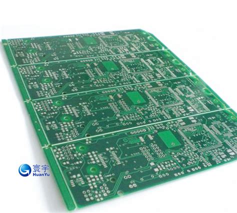
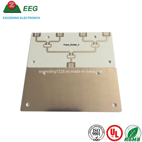
Single-sided PCBs, the simplest form, have components and traces on one side of the board. These are typically used in low-cost, low-density applications. Double-sided PCBs, on the other hand, have traces on both sides, allowing for more complex circuits and higher component density. For even more sophisticated applications, multi-layer PCBs are employed. These consist of multiple layers of substrate and traces, stacked and bonded together, enabling the design of highly complex circuits with increased functionality and performance.
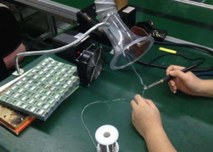
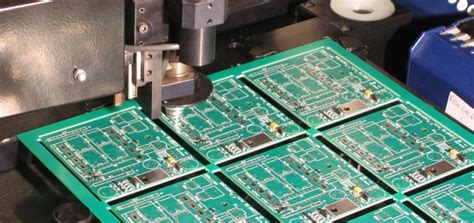
The manufacturing process of PCBs is a meticulous and precise endeavor, involving several stages to ensure the board’s quality and functionality.
Initially, the design of the PCB is created using specialized software, which outlines the layout of components and traces. This design is then transferred onto the board material through a process called photolithography, where a photoresist layer is applied and exposed to ultraviolet light to etch the desired pattern. Following this, the board undergoes a series of chemical treatments to remove excess copper, leaving only the intended traces. Finally, components are mounted onto the board through soldering, completing the assembly process.
In addition to their structural and functional attributes, PCBs are also subject to various standards and regulations to ensure their safety and reliability.
Organizations such as the Institute for Printed Circuits (IPC) establish guidelines for PCB design, manufacturing, and testing, ensuring that these components meet industry standards. Compliance with these standards is crucial, as it guarantees the performance and durability of electronic devices in which PCBs are used.
In conclusion, Printed Circuit Boards are integral to the functionality and advancement of modern electronic devices. Their ability to efficiently connect and support electronic components has made them a cornerstone of the electronics industry. Understanding the basics of PCBs, from their structure and types to their manufacturing process and regulatory standards, provides valuable insight into their critical role in today’s technology-driven world. As technology continues to evolve, the importance of PCBs in enabling innovation and enhancing device performance remains ever significant.
The Evolution Of Printed Circuit Boards: From Inception To Modern Day
Printed circuit boards (PCBs) have become an integral component of modern electronic devices, serving as the backbone that supports and connects various electronic components. The evolution of PCBs from their inception to the present day is a fascinating journey that highlights the rapid advancements in technology and manufacturing processes. Initially, electronic circuits were constructed using point-to-point wiring, a labor-intensive and error-prone method. This approach involved manually connecting each component with wires, which often resulted in unreliable connections and limited the complexity of the circuits that could be built.
The need for a more efficient and reliable method of constructing electronic circuits led to the development of the printed circuit board.
The concept of a PCB was first introduced in the early 20th century, with the invention of the printed wiring board by Albert Hanson in 1903. However, it was not until the 1940s that PCBs began to gain widespread use, particularly during World War II, when they were employed in military radios and other equipment. The introduction of the PCB marked a significant shift in electronic design, as it allowed for the mass production of complex circuits with greater reliability and consistency.
As technology continued to advance, so too did the design and manufacturing processes of PCBs.
The development of new materials and techniques, such as the use of fiberglass-reinforced epoxy laminates and photolithography, enabled the production of smaller, more intricate circuit patterns. This evolution was further accelerated by the advent of the integrated circuit in the 1960s, which necessitated even more compact and efficient PCB designs to accommodate the increasing number of components in electronic devices.
The miniaturization of electronic components and the demand for more powerful and versatile devices have driven continuous innovation in PCB technology.
Today, PCBs are available in a variety of types, including single-sided, double-sided, and multilayer boards, each offering different levels of complexity and functionality. Multilayer PCBs, in particular, have become essential in modern electronics, as they allow for the integration of numerous layers of circuitry within a single board, thereby maximizing space and performance.
Moreover, the rise of surface mount technology (SMT) has revolutionized PCB assembly by enabling components to be mounted directly onto the surface of the board,
rather than being inserted through holes. This advancement has not only reduced the size and weight of electronic devices but also improved their performance and reliability. Additionally, the use of computer-aided design (CAD) software has streamlined the PCB design process, allowing engineers to create highly complex and precise circuit layouts with ease.
In recent years, the focus on sustainability and environmental impact has also influenced the evolution of PCBs.
Manufacturers are increasingly adopting eco-friendly materials and processes, such as lead-free soldering and the use of biodegradable substrates, to reduce the environmental footprint of PCB production. Furthermore, the development of flexible and rigid-flex PCBs has opened up new possibilities for innovative electronic designs, enabling the creation of devices with unique form factors and enhanced functionality.
In conclusion, the evolution of printed circuit boards from their inception to the modern day is a testament to the relentless pursuit of innovation in the field of electronics. As technology continues to advance, PCBs will undoubtedly play a crucial role in shaping the future of electronic devices, driving further advancements in performance, efficiency, and sustainability.

Key Components Of A Printed Circuit Board: A Comprehensive Guide
A printed circuit board (PCB) is a fundamental component in modern electronic devices, serving as the backbone that supports and connects various electronic components. Understanding the key components of a PCB is essential for anyone involved in electronics design or manufacturing. At its core, a PCB is composed of a non-conductive substrate, typically made from fiberglass or composite epoxy, which provides structural support. This substrate is layered with conductive pathways, usually made of copper, that facilitate the flow of electrical signals between components.
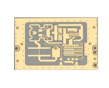
One of the primary components of a PCB is the trace, which is a thin line of conductive material that connects different parts of the circuit.
Traces are meticulously designed to ensure efficient signal transmission while minimizing interference and resistance. The width and thickness of these traces are crucial, as they must accommodate the current load without overheating or causing signal degradation. In addition to traces, vias are another critical element. Vias are small holes drilled through the PCB that allow electrical connections between different layers of the board. These are filled or plated with conductive material to ensure a reliable connection.
Moreover, pads are essential features on a PCB, providing the surface area where components are soldered.
These pads are strategically placed to align with the leads or terminals of electronic components, ensuring a secure and stable connection. The arrangement and size of pads are carefully designed to accommodate various component packages, such as surface-mount devices (SMDs) or through-hole components. The choice between these two types of components often depends on the specific application and manufacturing process.
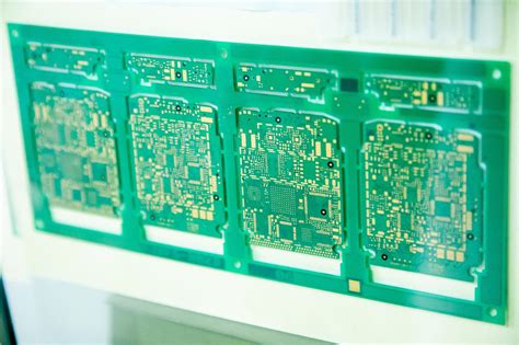
In addition to these structural elements, a PCB also includes a solder mask, which is a protective layer applied over the copper traces.
This mask prevents accidental short circuits and corrosion by insulating the conductive pathways. Typically green, though available in various colors, the solder mask also aids in the soldering process by keeping solder confined to the pads. Complementing the solder mask is the silkscreen layer, which provides printed information on the PCB, such as component labels, reference designators, and other identifiers. This layer is crucial for assembly and troubleshooting, as it helps technicians and engineers quickly identify components and their orientation.
Furthermore, the integration of electronic components is a vital aspect of PCB design.
These components, which include resistors, capacitors, diodes, and integrated circuits, are mounted onto the board and connected via the traces and pads. Each component serves a specific function within the circuit, contributing to the overall operation of the electronic device. The placement and orientation of these components are meticulously planned to optimize performance and minimize potential issues such as electromagnetic interference.
In conclusion, the key components of a printed circuit board work in harmony to create a functional and efficient electronic circuit. From the conductive traces and vias to the protective solder mask and informative silkscreen, each element plays a crucial role in the overall design and functionality of the PCB. Understanding these components and their interactions is essential for anyone involved in the design, manufacturing, or repair of electronic devices, as it ensures the creation of reliable and high-performing products.
The Role Of Printed Circuit Boards In Modern Electronics
Printed circuit boards (PCBs) are fundamental components in the realm of modern electronics, serving as the backbone for most electronic devices. These intricate boards are designed to mechanically support and electrically connect electronic components using conductive pathways, tracks, or signal traces etched from copper sheets laminated onto a non-conductive substrate. The evolution of PCBs has been pivotal in the miniaturization and enhancement of electronic devices, making them indispensable in today’s technology-driven world.
To understand the role of PCBs, it is essential to recognize their function in electronic devices.
At the core, PCBs provide a platform for mounting various electronic components such as resistors, capacitors, and integrated circuits. By organizing these components in a compact and efficient manner, PCBs facilitate the seamless flow of electrical signals, ensuring that devices operate as intended. This organization not only enhances the reliability of electronic devices but also contributes to their longevity by reducing the risk of short circuits and other electrical failures.
Moreover, the versatility of PCBs allows them to be customized for a wide range of applications, from simple consumer electronics to complex industrial machinery.
For instance, in consumer electronics like smartphones and laptops, PCBs are designed to accommodate high-density component placement, enabling the production of sleek and lightweight devices. In contrast, industrial applications may require PCBs that can withstand harsh environmental conditions, necessitating the use of robust materials and specialized coatings.
The manufacturing process of PCBs is a meticulous one, involving several stages to ensure precision and quality.
Initially, a PCB design is created using computer-aided design (CAD) software, which outlines the layout of the board and the placement of components. This design is then transferred onto a physical board through a series of processes, including etching, drilling, and plating. Each step is critical, as even minor errors can lead to significant malfunctions in the final product. Consequently, rigorous testing is conducted to verify the functionality and reliability of the PCBs before they are integrated into electronic devices.
In addition to their structural and functional roles, PCBs also contribute to the sustainability of electronic devices.
By enabling the efficient use of materials and reducing the need for extensive wiring, PCBs help minimize electronic waste. Furthermore, advancements in PCB technology have led to the development of environmentally friendly materials and manufacturing processes, aligning with global efforts to promote sustainable practices in the electronics industry.
As technology continues to advance, the role of PCBs is expected to expand further.
Emerging trends such as the Internet of Things (IoT), wearable technology, and smart devices demand increasingly sophisticated PCBs that can support complex functionalities while maintaining compact form factors. This ongoing evolution underscores the importance of continued innovation in PCB design and manufacturing, ensuring that they remain at the forefront of technological progress.
In conclusion, printed circuit boards are integral to the functionality and advancement of modern electronics. Their ability to support and connect electronic components efficiently has revolutionized the way devices are designed and manufactured. As the demand for more advanced and sustainable electronic solutions grows, the role of PCBs will undoubtedly become even more critical, driving further innovation and shaping the future of technology.