Assembled PCB Manufacturing: Precision Techniques for Modern Electronics

Key Takeaways
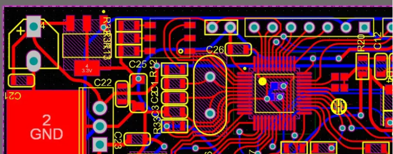
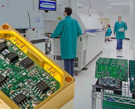
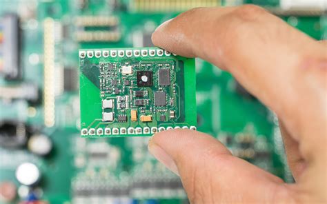
Modern PCB assembly processes rely on automated systems to achieve millimeter-level accuracy, ensuring consistency across high-volume production. From PCBA design validation to final inspection, precision is maintained through advanced tools like automated optical inspection (AOI) and laser-aligned pick-and-place machines.
A critical advancement lies in surface mount technology (SMT), which enables the placement of ultra-compact components with tolerances under 0.1mm. This method, combined with lead-free soldering techniques, meets stringent environmental regulations while enhancing thermal resilience.
| Technique | Purpose | Tolerance |
|---|---|---|
| Laser Drilling | Microvia creation for HDI boards | ±10μm |
| Reflow Soldering | Component attachment | ±2°C control |
| AOI Systems | Defect detection | 99.98% accuracy |
Quality assurance protocols, such as in-circuit testing (ICT) and functional validation, ensure circuit board reliability under extreme conditions. Emerging materials like polyimide substrates and ceramic-filled laminates further improve thermal management, critical for applications in aerospace and automotive industries.
The integration of AI-driven analytics in PCBA workflows optimizes defect prediction, reducing rework rates by up to 40%. As miniaturization trends accelerate, innovations in 3D printing and embedded component technology are redefining the boundaries of PCB assembly efficiency.
Automated Systems in PCB Assembly
Modern PCB assembly workflows rely heavily on automated systems to achieve the speed and accuracy required for high-volume production. Robotic pick-and-place machines, equipped with vision-guided alignment, position surface-mount components with micron-level precision, reducing human error by over 90%. These systems integrate seamlessly with automated optical inspection (AOI) tools, which scan solder joints and component placements in real time, flagging defects like tombstoning or bridging before boards advance to subsequent stages.
Tip: For mixed-technology PCBA lines, synchronized automation between through-hole insertion machines and reflow ovens ensures consistent thermal profiles across hybrid designs.
Advanced conveyor systems now incorporate machine learning algorithms to optimize throughput, dynamically adjusting feed rates based on component complexity. Closed-loop feedback mechanisms in automated solder paste dispensers maintain precise deposition volumes, critical for micro-BGA and QFN packages. The shift toward Industry 4.0-compliant assembly cells enables remote monitoring of key metrics like cycle times and defect ratios, allowing manufacturers to preemptively address process deviations.
As PCB assembly scales to meet 5G and IoT demands, collaborative robots (cobots) are increasingly deployed for flexible low-to-mid volume production. These systems retain traceability through embedded RFID tagging, aligning with IPC-A-610 standards while cutting rework costs by 40-60%. The integration of automation not only accelerates PCBA timelines but also elevates repeatability in creating mission-critical electronics.
Precision Soldering Techniques Explained
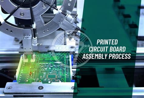
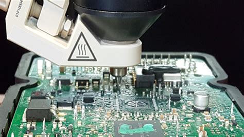
PCB assembly relies heavily on precision soldering to ensure electrical continuity and mechanical stability in modern electronics. Unlike traditional methods, contemporary surface-mount technology (SMT) demands micron-level accuracy, particularly when integrating miniaturized components. Advanced PCBA processes employ reflow soldering, where controlled heat profiles melt solder paste uniformly, creating reliable connections without damaging sensitive parts. For through-hole components, selective soldering systems target specific areas, reducing thermal stress on adjacent elements.
Critical to these techniques is the use of nitrogen-assisted environments, which minimize oxidation during soldering, enhancing joint integrity. Automated optical inspection (AOI) systems then verify solder quality, flagging issues like voiding or cold joints for correction. Manufacturers increasingly adopt lead-free alloys (e.g., SAC305) to meet environmental standards while maintaining performance. These innovations underscore how precision soldering balances speed and reliability in high-volume PCB assembly, directly impacting the durability of end-use electronics.
Quality Control for Circuit Board Reliability
Ensuring reliability in PCB assembly requires a multilayered approach to quality control. Automated optical inspection (AOI) systems scan microscopic defects like solder bridging or misaligned components, while X-ray inspection verifies hidden connections in ball grid arrays (BGAs) and multilayer boards. For PCBA units destined for high-stress environments, thermal cycling tests simulate extreme temperature fluctuations to identify potential material fatigue.
Advanced electrical testing protocols, including in-circuit testing (ICT) and flying probe measurements, validate circuit continuity and functional performance against design specifications. Manufacturers increasingly integrate statistical process control (SPC) software to monitor production trends, enabling real-time adjustments to soldering profiles or component placement accuracy. Cross-sectional analysis and ion chromatography further detect voids in solder joints or ionic contamination that could compromise long-term stability.
To maintain consistency, leading PCB assembly providers enforce material traceability systems aligned with IPC-1782 standards, ensuring every layer, laminate, and solder alloy meets certified specifications. This rigorous framework not only reduces field failure rates but also supports compliance with automotive (IATF 16949) and aerospace (AS9100D) reliability benchmarks for PCBA applications.
Advanced Materials in Modern PCB Manufacturing
The evolution of PCB assembly processes hinges on breakthroughs in material science, enabling higher performance and reliability in modern electronics. Today’s PCBA designs leverage high-frequency laminates like Rogers 4000 series, which minimize signal loss in 5G and IoT applications, while thermal management substrates such as aluminum-clad or ceramic-filled boards dissipate heat more efficiently. Innovations in halogen-free flame-retardant materials align with environmental regulations without compromising durability.
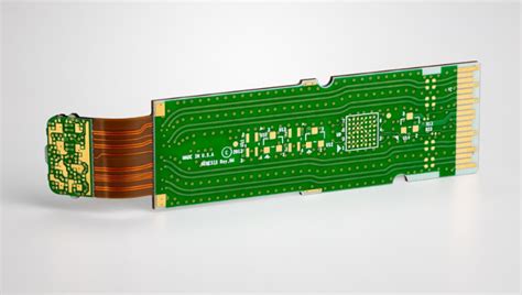
A critical shift involves the adoption of low-loss dielectrics for high-speed circuits, ensuring signal integrity in advanced computing systems. Flexible polyimide films are increasingly used in wearable devices, allowing bendable PCB assembly without cracking conductive traces. For harsh environments, thermally conductive adhesives and coatings protect components from moisture and mechanical stress.
Material compatibility with laser drilling and surface mount technology is also prioritized, ensuring seamless integration into automated production lines. Manufacturers now balance cost-effectiveness with performance by layering standard FR-4 cores with specialized materials in hybrid designs. These advancements not only enhance PCBA longevity but also pave the way for next-generation miniaturized electronics, where material properties directly define functional boundaries.
Laser Technology for Accurate PCB Drilling
Modern PCB assembly relies on laser drilling systems to achieve micron-level precision in creating via holes—critical for high-density interconnect (HDI) designs. Unlike mechanical drilling, fiber lasers eliminate tool wear and material stress, enabling diameters as small as 25µm while maintaining ±5µm positional accuracy. This capability is particularly crucial for PCBA involving multilayer boards, where misaligned vias can disrupt signal integrity or cause thermal failures.
Advanced laser systems utilize ultraviolet (UV) wavelengths to vaporize copper and dielectric materials cleanly, reducing debris and minimizing post-processing. Real-time optical calibration ensures alignment with CAD designs, even when processing flexible substrates or heat-sensitive laminates. To ensure consistency, manufacturers integrate automated inspection tools that measure hole wall roughness and taper angles, flagging deviations before components are mounted.
By integrating laser drilling into PCB assembly workflows, producers achieve tighter tolerances required for 5G devices, wearables, and automotive electronics. The technique’s scalability also supports rapid prototyping in PCBA, allowing engineers to test complex layouts without retooling mechanical drills. As board densities increase, laser technology remains indispensable for balancing precision with cost-effective mass production.
Surface Mount Technology Implementation Guide
Implementing Surface Mount Technology (SMT) requires meticulous planning to ensure seamless integration into PCB assembly workflows. Unlike traditional through-hole methods, SMT enables high-density component placement by mounting devices directly onto the board’s surface. This approach enhances PCBA efficiency, particularly for compact, high-performance electronics like smartphones or IoT devices.
The process begins with stencil preparation, where laser-cut templates deposit precise amounts of solder paste onto designated pads. Automated pick-and-place machines then position surface-mount devices (SMDs)—such as resistors, capacitors, and ICs—with micron-level accuracy. These systems rely on vision alignment technologies to compensate for minor board irregularities, ensuring consistent placement across high-volume production runs.
A critical phase involves reflow soldering, where boards pass through controlled thermal zones to melt solder paste without damaging sensitive components. Optimizing thermal profiles prevents issues like tombstoning or cold joints, which compromise circuit board reliability. Post-soldering, automated optical inspection (AOI) systems scan for defects such as misaligned components or insufficient solder, while X-ray inspection verifies hidden connections in multilayer designs.
Integrating SMT into PCB assembly workflows demands compatibility with advanced materials like low-temperature solder alloys and high-frequency substrates. As miniaturization trends accelerate, manufacturers must balance precision with scalability—leveraging SMT’s advantages while maintaining rigorous quality control protocols to meet evolving industry standards.

Testing Protocols for Durable Electronics
Rigorous testing protocols form the backbone of reliable PCB assembly, ensuring end products withstand operational stresses and environmental challenges. Modern PCBA workflows integrate automated optical inspection (AOI) and X-ray inspection (AXI) to detect microscopic defects like solder bridging or component misalignment. These systems validate alignment with IPC-A-610 standards, critical for aerospace and automotive applications where failure risks are unacceptable.
Environmental stress testing simulates real-world conditions, exposing boards to extreme temperatures, humidity, and vibration cycles. Thermal cycling tests, for instance, assess material expansion tolerances, while electrical continuity checks verify signal integrity under load. For high-density designs, boundary scan testing identifies open or short circuits in complex interconnect architectures.
Advanced PCB assembly lines now incorporate machine learning algorithms to analyze test data, predicting failure patterns before mass production. This proactive approach reduces rework rates by up to 40% in PCBA workflows. Additionally, in-circuit testing (ICT) ensures components like capacitors and resistors meet specified parameters, bridging quality assurance between prototyping and full-scale manufacturing.
By harmonizing these protocols with evolving industry demands, manufacturers achieve the durability benchmarks required for next-generation IoT devices and industrial automation systems.
Future Trends in PCB Production Innovation
The evolution of PCB assembly processes is being reshaped by emerging technologies that prioritize efficiency, miniaturization, and environmental sustainability. Industry 4.0 integration is driving the adoption of smart factories, where IoT-enabled equipment and AI-powered analytics optimize PCBA workflows in real time. Additive manufacturing techniques, such as 3D-printed conductive traces, are reducing material waste while enabling complex, high-density designs. Innovations like embedded component technology—where passive elements are laminated within the board itself—are pushing the boundaries of compact, high-performance electronics.
Advanced materials, including low-loss dielectrics and recyclable substrates, are gaining traction to meet both performance demands and regulatory requirements for eco-conscious manufacturing. Meanwhile, laser-direct structuring (LDS) and modular PCB assembly systems are accelerating prototyping cycles, allowing faster adaptation to market needs. The rise of flexible hybrid electronics (FHE) further underscores the shift toward bendable, lightweight solutions for wearable devices and IoT applications.
As automation merges with machine learning, predictive maintenance and self-correcting assembly lines are becoming standard, minimizing human intervention while maximizing yield. These advancements position PCBA as a cornerstone for next-generation innovations, from quantum computing modules to energy-efficient smart grids.
Conclusion
The evolution of PCB assembly processes underscores the critical balance between precision engineering and scalable manufacturing in modern electronics. As industries demand higher performance in compact form factors, PCBA workflows have embraced innovations such as automated optical inspection and laser-etched trace alignment to ensure micron-level accuracy. These advancements, coupled with rigorous thermal stress testing, directly address the reliability requirements of applications ranging from consumer devices to aerospace systems.
Looking ahead, the integration of AI-driven defect detection and sustainable material sourcing will further refine PCB assembly standards. Manufacturers prioritizing end-to-end traceability and flexible prototyping are poised to lead in markets where rapid iteration and compliance with environmental regulations are non-negotiable. For PCBA providers, the focus remains on harmonizing cutting-edge techniques like 3D-printed circuitry with cost-effective production models—a strategy that ensures both technological leadership and commercial viability in an increasingly interconnected world.
FAQs
What distinguishes PCB assembly from PCBA?
PCB assembly refers to the process of populating a bare circuit board with components, while PCBA (Printed Circuit Board Assembly) denotes the fully assembled and functional board ready for integration into electronic devices. The latter includes rigorous testing to ensure operational reliability.
How does automated optical inspection enhance quality control?
Modern pcb assembly lines employ automated optical inspection (AOI) systems to detect soldering defects, component misalignment, and trace imperfections. This technology reduces human error, ensuring consistent adherence to IPC-A-610 standards for PCBA reliability.
What materials influence thermal management in high-density boards?
Advanced substrates like polyimide flex materials and ceramic-filled laminates improve heat dissipation in compact pcb assembly designs. These materials maintain stability under high-frequency operation, critical for aerospace and medical electronics.
Why is laser drilling preferred for microvia formation?
Laser drilling achieves precision holes as small as 25µm, enabling multilayer interconnects in high-density PCBA designs. This method minimizes mechanical stress, enhancing signal integrity in 5G and IoT applications.
How does surface mount technology optimize production scalability?
SMT allows rapid placement of miniature components using pick-and-place machines, reducing pcb assembly time by up to 70%. Its compatibility with reflow soldering ensures uniform joints, vital for mass-producing wearables and automotive systems.
Explore Professional PCB Assembly Solutions
For tailored pcb assembly services integrating cutting-edge technologies, please click here to consult our engineering team.