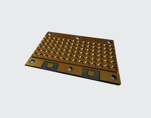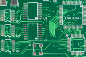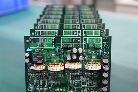
Assembly outline pcb
Understanding The Basics Of Assembly Outline PCB Design
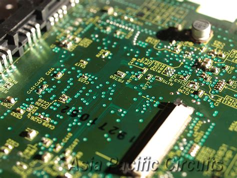
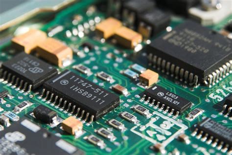
In the realm of electronics manufacturing, understanding the basics of assembly outline PCB (Printed Circuit Board) design is crucial for ensuring the successful production of electronic devices. The assembly outline serves as a blueprint that guides the manufacturing process, providing essential information about the layout and components of the PCB. This foundational knowledge is indispensable for engineers and designers who aim to create efficient and reliable electronic products.
To begin with, the assembly outline of a PCB is a detailed representation of the board’s physical dimensions and the placement of its components.
It includes critical information such as the board’s shape, size, and the location of mounting holes, which are essential for fitting the PCB into its intended enclosure. Additionally, the outline specifies the positions of various components, such as resistors, capacitors, and integrated circuits, ensuring that each element is correctly placed for optimal functionality. This meticulous planning is vital, as even minor errors in component placement can lead to significant issues in the final product.
Moreover, the assembly outline is not just a static diagram; it is a dynamic tool that evolves throughout the design process.
Initially, it serves as a conceptual framework that helps designers visualize the overall layout of the PCB. As the design progresses, the outline becomes more detailed, incorporating specific component footprints and routing paths.
This iterative process allows designers to refine their designs, making necessary adjustments to improve performance and manufacturability.
By continuously updating the assembly outline, designers can identify potential issues early in the design phase, reducing the risk of costly revisions later on.
In addition to its role in design, the assembly outline is also a critical component of the manufacturing process.
It provides manufacturers with the information needed to assemble the PCB accurately and efficiently. For instance, the outline includes details about the orientation of components, which is crucial for automated assembly machines that rely on precise positioning to place components correctly.
Furthermore, the outline may include notes on specific assembly instructions, such as the need for certain components to be hand-soldered or the use of particular soldering techniques. These instructions ensure that the PCB is assembled according to the designer’s specifications, maintaining the integrity and performance of the final product.
Transitioning from design to production, the assembly outline also plays a vital role in quality control.
By providing a comprehensive overview of the PCB’s layout and components, the outline serves as a reference point for inspecting the assembled board. Quality control personnel can use the outline to verify that all components are present and correctly placed, ensuring that the PCB meets the required standards. This verification process is essential for identifying defects and preventing faulty products from reaching the market.
In conclusion, the assembly outline is an indispensable element of PCB design and manufacturing. It provides a detailed roadmap that guides the entire process, from initial design to final production. By understanding the basics of assembly outline PCB design, engineers and designers can create more efficient and reliable electronic products, ultimately contributing to the advancement of technology. As the electronics industry continues to evolve, the importance of a well-crafted assembly outline cannot be overstated, serving as a cornerstone for innovation and quality in PCB design.
Key Considerations For Effective Assembly Outline PCB Layout
When designing an assembly outline for a printed circuit board (PCB), several key considerations must be taken into account to ensure an effective and efficient layout. The assembly outline serves as a critical guide for the manufacturing and assembly processes, providing essential information about the board’s dimensions, component placements, and other vital specifications. Therefore, understanding the nuances of creating a precise and comprehensive assembly outline is crucial for engineers and designers aiming to optimize the functionality and manufacturability of their PCBs.
To begin with, the accuracy of the board dimensions is paramount.
The assembly outline must clearly define the PCB’s physical boundaries, including its length, width, and thickness. This information is essential not only for the fabrication process but also for ensuring that the board fits correctly within its intended enclosure or system. Any discrepancies in these measurements can lead to significant issues during assembly, potentially resulting in costly redesigns or adjustments. Therefore, meticulous attention to detail is required when specifying these dimensions.
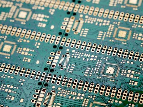
In addition to the board’s physical dimensions, the placement of components within the assembly outline is another critical consideration.
Components must be strategically positioned to optimize both electrical performance and manufacturability. This involves considering factors such as signal integrity, thermal management, and ease of assembly.
For instance, high-speed components should be placed in proximity to minimize signal path lengths, while heat-generating components may require strategic placement to facilitate effective heat dissipation. Furthermore, ensuring that components are accessible for assembly and testing can significantly streamline the manufacturing process.
Transitioning from component placement, the assembly outline must also account for the routing of traces and vias.
Efficient routing is essential to maintain signal integrity and minimize electromagnetic interference. Designers should aim to create a layout that reduces the length of critical signal paths and avoids unnecessary bends or loops. Additionally, the use of ground planes and power planes can help to further enhance signal integrity and reduce noise. By carefully planning the routing within the assembly outline, designers can ensure that the PCB performs optimally in its intended application.
Moreover, the assembly outline should include detailed information about the board’s layers and stack-up.
This includes specifying the number of layers, the materials used, and the thickness of each layer. Such information is crucial for both the fabrication and assembly processes, as it impacts factors such as impedance control and thermal performance. A well-defined layer stack-up can also aid in achieving the desired electrical characteristics and ensuring the board’s reliability under various operating conditions.
Finally, it is important to consider the inclusion of fiducial markers and tooling holes within the assembly outline.
Fiducial markers serve as reference points for automated assembly equipment, ensuring precise alignment and placement of components. Tooling holes, on the other hand, facilitate the handling and alignment of the PCB during the manufacturing process. Including these features in the assembly outline can significantly enhance the efficiency and accuracy of the assembly process.
In conclusion, creating an effective assembly outline for a PCB layout involves careful consideration of various factors, including board dimensions, component placement, trace routing, layer stack-up, and the inclusion of fiducial markers and tooling holes.
By addressing these key considerations, designers can ensure that their PCBs are not only functional and reliable but also manufacturable and cost-effective. Through meticulous planning and attention to detail, the assembly outline can serve as a vital tool in guiding the successful production of high-quality printed circuit boards.
Common Challenges In Assembly Outline PCB Manufacturing
In the realm of electronics manufacturing, the assembly outline of printed circuit boards (PCBs) plays a crucial role in ensuring the functionality and reliability of electronic devices. However, the process of manufacturing PCBs is fraught with challenges that can impact both the efficiency and quality of the final product. Understanding these common challenges is essential for manufacturers aiming to optimize their production processes and deliver high-quality PCBs.
One of the primary challenges in PCB assembly outline manufacturing is the complexity of design specifications.
As electronic devices become more sophisticated, the demand for intricate PCB designs has increased. This complexity often leads to difficulties in translating design specifications into manufacturable products. For instance, the need for precise alignment of multiple layers in multilayer PCBs can pose significant challenges.
Misalignment can result in electrical failures or reduced performance, necessitating meticulous attention to detail during the manufacturing process.
Moreover, the miniaturization of electronic components further complicates the assembly outline process.
As components become smaller, the margin for error decreases, requiring advanced techniques and equipment to ensure accurate placement and soldering. This miniaturization trend also demands higher precision in the etching and drilling processes, as even minor deviations can lead to significant issues in the final product.
Consequently, manufacturers must invest in state-of-the-art technology and skilled personnel to meet these stringent requirements.
In addition to design and miniaturization challenges, material selection is another critical factor in PCB manufacturing.
The choice of materials affects not only the performance but also the durability and cost of the PCB. Manufacturers must carefully consider factors such as thermal conductivity, dielectric properties, and mechanical strength when selecting materials.
Inadequate material selection can lead to issues such as delamination, warping, or thermal failure, which can compromise the integrity of the PCB.
Furthermore, the soldering process presents its own set of challenges. Achieving a reliable solder joint is essential for the electrical connectivity and mechanical stability of the PCB. However, factors such as solder paste composition, reflow temperature profiles, and component placement accuracy can all influence the quality of the solder joints. Manufacturers must meticulously control these variables to prevent defects such as cold solder joints, bridging, or tombstoning, which can lead to device failure.
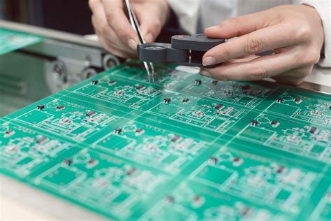
Another significant challenge in PCB assembly outline manufacturing is the need for rigorous testing and quality assurance.
Given the critical role that PCBs play in electronic devices, ensuring their reliability is paramount. Manufacturers must implement comprehensive testing protocols to identify and rectify defects before the PCBs reach the end user.
This often involves a combination of visual inspections, automated optical inspections, and functional testing. However, the complexity of modern PCBs can make thorough testing a time-consuming and costly endeavor.
Finally, environmental and regulatory considerations add another layer of complexity to PCB manufacturing.
Manufacturers must comply with various regulations, such as the Restriction of Hazardous Substances (RoHS) directive, which limits the use of certain hazardous materials in electronic products. Adhering to these regulations requires careful selection of materials and processes, which can increase production costs and complexity.
In conclusion, the assembly outline of PCBs is a critical aspect of electronics manufacturing that presents numerous challenges. From complex design specifications and miniaturization to material selection and soldering, each step in the process requires careful consideration and precision. By understanding and addressing these challenges, manufacturers can enhance the quality and reliability of their PCBs, ultimately contributing to the success of the electronic devices they power.
Innovative Techniques In Assembly Outline PCB Prototyping
In the rapidly evolving field of electronics, the demand for efficient and precise assembly outline PCB (Printed Circuit Board) prototyping has never been more critical. As technology advances, so too do the methods and techniques employed in the creation of these essential components. Innovative techniques in assembly outline PCB prototyping are transforming the landscape, offering enhanced precision, reduced production times, and increased flexibility in design. These advancements are not only meeting the growing demands of the industry but are also setting new standards for quality and efficiency.
One of the most significant innovations in PCB prototyping is the adoption of automated processes.
Automation has revolutionized the way PCBs are designed and assembled, allowing for greater accuracy and consistency. By utilizing computer-aided design (CAD) software, engineers can create highly detailed and precise PCB layouts. This software enables the simulation of various design scenarios, ensuring that potential issues are identified and addressed before the physical prototyping stage. Consequently, this reduces the likelihood of errors and minimizes the need for costly revisions.
Moreover, the integration of 3D printing technology into PCB prototyping has opened new avenues for innovation.
3D printing allows for the rapid production of complex PCB designs that would be challenging to achieve using traditional methods. This technology not only accelerates the prototyping process but also provides greater flexibility in design, enabling engineers to experiment with novel configurations and materials. As a result, 3D printing is becoming an indispensable tool in the development of next-generation electronic devices.
In addition to automation and 3D printing, the use of advanced materials is another area where significant progress is being made.
Traditional PCBs are typically made from fiberglass-reinforced epoxy laminate, but recent advancements have introduced alternative materials such as flexible polymers and ceramics. These materials offer unique properties, such as increased thermal conductivity and flexibility, which can enhance the performance and durability of the final product. By incorporating these advanced materials into the prototyping process, engineers can create PCBs that are better suited to the specific requirements of modern electronic devices.
Furthermore, the implementation of machine learning algorithms in PCB prototyping is an emerging trend that holds great promise.
Machine learning can analyze vast amounts of data to identify patterns and optimize design parameters, leading to more efficient and effective prototyping processes. By leveraging these algorithms, engineers can predict potential design flaws and optimize the layout for improved performance. This not only streamlines the prototyping process but also results in higher-quality PCBs that meet the stringent demands of today’s technology-driven world.
As these innovative techniques continue to evolve, the future of assembly outline PCB prototyping looks increasingly promising.
The combination of automation, 3D printing, advanced materials, and machine learning is paving the way for more efficient, precise, and flexible prototyping processes. These advancements are not only enhancing the capabilities of engineers and designers but are also driving the development of cutting-edge electronic devices that are shaping the future of technology. As the industry continues to embrace these innovations, the potential for further breakthroughs in PCB prototyping is vast, promising a future where the boundaries of what is possible are continually expanded.