Automated Circuit Board Assembly: Precision in Electronics Production
Key Takeaways
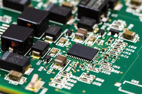
Modern PCB assembly processes leverage precision engineering to achieve tolerances under 25 microns, ensuring consistent performance in high-density electronics. PCBA systems now integrate machine vision and AI-driven algorithms to execute error-free component placement, reducing defects by up to 99.7% compared to manual methods.
Tip: Regular calibration of robotic placement systems maintains micron-level accuracy across high-volume production runs.
The shift toward automated circuit board assembly has accelerated production cycles by 60-80%, with advanced pick-and-place robots achieving speeds exceeding 25,000 components per hour. Innovations like 3D solder paste inspection and real-time thermal profiling further enhance reliability in PCB fabrication. Notably, recent collaborations in supply chain automation, such as Boardera and CoFactr’s initiative, demonstrate how integrated systems can reduce lead times by 30-40%.
Cost-efficiency improvements stem from predictive maintenance protocols and closed-loop feedback systems, which minimize downtime and material waste. In smart factories, IoT-enabled PCBA lines synchronize with quality control databases, enabling zero-defect manufacturing targets. These developments underscore how robotics and AI are not merely augmenting but fundamentally redefining electronics manufacturing standards.
Precision Engineering in PCB Automation
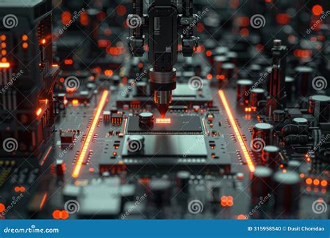
Modern PCB assembly processes rely on advanced precision engineering to achieve sub-micron alignment accuracy in component placement. Automated systems integrate PCBA-optimized workflows, combining high-speed robotics with machine vision to verify component orientation and solder paste application. These technologies eliminate human error, ensuring error-free component placement even for micro-BGA packages or 01005-sized passives.
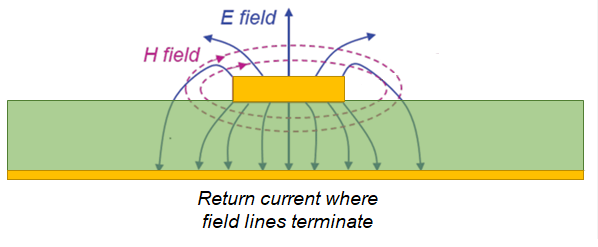
A critical innovation lies in real-time feedback loops, where sensors detect deviations during PCB assembly and trigger immediate corrections. For example, automated optical inspection (AOI) systems scan boards at 20+ megapixel resolution, flagging defects like tombstoning or skewed capacitors before reflow soldering. This precision is further enhanced by laser-guided pick-and-place machines, which achieve placement speeds exceeding 50,000 components per hour while maintaining ±25μm positional accuracy.
| Parameter | Manual Assembly | Automated PCBA |
|---|---|---|
| Placement Accuracy | ±500μm | ±25μm |
| Defect Rate | 1,200 PPM | <50 PPM |
| Throughput (CPH) | 800 | 50,000+ |
Such advancements enable manufacturers to meet stringent aerospace and medical device standards, where thermal management and signal integrity depend on exact component positioning. By harmonizing precision engineering with PCB assembly automation, industries achieve repeatable quality while scaling production to meet global electronics demand.
Error-Free Component Placement Techniques
Modern PCB assembly processes rely on advanced technologies to achieve sub-micron accuracy in component placement, ensuring PCBA outcomes meet stringent quality benchmarks. Automated optical inspection (AOI) systems, integrated with machine vision algorithms, verify component alignment in real time, identifying deviations as small as 0.01mm. These systems work in tandem with high-speed pick-and-place robots, which utilize vacuum nozzles and servo motors to position surface-mount devices (SMDs) at rates exceeding 25,000 components per hour.
A critical innovation lies in closed-loop feedback mechanisms, where data from AOI scanners instantly adjusts robotic placement parameters, minimizing rework. For instance, a recent implementation in network communication hardware demonstrated a 99.998% placement accuracy across 10,000 boards. Additionally, AI-driven predictive modeling anticipates thermal expansion effects during soldering, further reducing misalignment risks.
The shift toward Industry 4.0-ready PCBA lines has introduced digital twin simulations, enabling engineers to pre-validate placement patterns before physical production. This approach not only eliminates human calibration errors but also accelerates setup times for mixed-product batches. As precision requirements intensify for miniaturized electronics, these error-mitigation strategies remain central to maintaining yield rates above 99.5% in high-volume manufacturing.
Accelerating Electronics Production Cycles
The demand for faster electronics manufacturing has made PCB assembly processes a critical focus area for industry leaders. Automated PCBA systems now achieve cycle time reductions of 40-60% compared to manual workflows, primarily through synchronized robotic arms and real-time calibration mechanisms. By integrating surface-mount technology (SMT) with high-speed pick-and-place machines, manufacturers can position up to 25,000 components per hour with micron-level accuracy—a feat unattainable in traditional setups.
Transitioning to automated workflows also minimizes bottlenecks caused by human-dependent tasks. For instance, advanced conveyor systems ensure seamless transfer between soldering, inspection, and testing stages, while machine learning algorithms optimize material flow. This acceleration is further amplified by predictive maintenance protocols, which preempt equipment downtime by analyzing performance data from sensors embedded in PCB assembly lines.
Notably, the shift toward lights-out manufacturing enables continuous production without manual intervention, slashing lead times for complex multilayer boards. As automated PCBA solutions evolve, industries ranging from consumer electronics to aerospace benefit from compressed development timelines—transforming weeks-long processes into matter-of-days operations. These advancements underscore how precision automation is redefining speed as a competitive advantage in electronics manufacturing.
Innovations Driving PCB Fabrication Tech
Modern advancements in PCB assembly (PCBA) technologies are reshaping electronics manufacturing through cutting-edge engineering solutions. The integration of additive manufacturing techniques, such as 3D-printed circuitry, allows for intricate designs that traditional methods cannot achieve. Laser direct imaging (LDI) systems now enable micron-level accuracy in trace patterning, ensuring flawless component alignment even in high-density boards. Additionally, AI-powered optical inspection tools automatically detect defects like soldering errors or misplaced components, reducing rework rates by up to 40%.
Another breakthrough lies in modular assembly lines, where robotic arms equipped with machine vision adapt to varying PCBA designs without manual recalibration. These systems leverage real-time data analytics to optimize throughput, aligning with the demand for faster production cycles. For instance, a recent instrumentation project demonstrated how adaptive automation reduced assembly time by 30% while maintaining zero-defect output. Furthermore, the adoption of IoT-enabled machinery creates interconnected workflows, allowing manufacturers to monitor PCB assembly processes remotely and predict maintenance needs. Such innovations not only enhance precision but also pave the way for scalable, smart factory ecosystems in electronics production.
Robotics Revolutionizing Circuit Assembly
Modern PCB assembly processes have undergone transformative changes with the integration of advanced robotics. Industrial robotic arms equipped with micro-precision actuators now handle PCBA tasks that once required manual dexterity, achieving placement accuracies within ±0.025mm. These systems utilize machine vision to align components on circuit boards at speeds exceeding 25,000 placements per hour, reducing human error by over 90%. By automating repetitive tasks such as solder paste application and surface-mount technology (SMT) placement, manufacturers can allocate skilled technicians to quality assurance roles, creating a symbiotic relationship between human expertise and robotic efficiency.
The adoption of collaborative robots (cobots) further enhances flexibility in production lines. Unlike traditional static machinery, cobots adapt to varying PCB assembly requirements through real-time programming adjustments, enabling rapid transitions between product batches. This agility is critical for industries demanding high-mix, low-volume production, such as aerospace and medical device manufacturing. Additionally, closed-loop feedback systems embedded in robotic workflows continuously monitor thermal profiles and solder joint integrity, ensuring compliance with PCBA reliability standards.
As factories transition toward Industry 4.0 frameworks, robotics-driven PCB assembly lines integrate with AI-powered analytics platforms. These systems predict maintenance needs and optimize material utilization, driving down waste while sustaining throughput. The result is a seamless fusion of mechanical precision and digital intelligence, redefining scalability in electronics manufacturing.
Automated Systems for Flawless PCBs
Modern PCB assembly processes rely on advanced automated systems to achieve near-perfect circuit board fabrication. By integrating robotic pick-and-place machines with machine vision systems, manufacturers ensure micron-level accuracy in component positioning—critical for high-density PCBA designs. These systems leverage real-time feedback loops to correct deviations, reducing defects to fewer than 15 parts per million (PPM) in optimized production lines.
A key innovation lies in closed-loop control mechanisms, which dynamically adjust parameters like solder paste deposition and thermal profiles during reflow soldering. For example, recent studies highlight how adaptive algorithms minimize tombstoning or bridging, particularly in micro-BGA and QFN packages. Furthermore, automated optical inspection (AOI) scanners perform 3D solder joint analysis at speeds exceeding 20,000 inspections per hour, flagging anomalies before boards advance to testing phases.
Such automation not only enhances precision but also standardizes outcomes across batches—a necessity for industries like aerospace and medical devices where reliability is non-negotiable. By eliminating human variability, these systems enable PCB assembly lines to maintain ISO 9001:2015 compliance while scaling production volumes. As factories adopt AI-driven predictive maintenance, downtime for PCBA equipment has dropped by 40%, reinforcing the role of automation in sustaining flawless manufacturing workflows.
Cost-Efficiency in Automated PCB Manufacturing
The adoption of automated PCB assembly systems has become a cornerstone for achieving cost-efficiency in modern electronics production. By integrating advanced PCBA (Printed Circuit Board Assembly) technologies, manufacturers reduce labor-intensive processes while minimizing material waste. Robotic placement systems, for instance, optimize component utilization by precisely allocating solder paste and parts, cutting excess consumption by up to 30% compared to manual methods. This precision also slashes error-related expenses, as automated optical inspection (AOI) systems detect defects early, preventing costly rework cycles.
Transitioning to automated workflows further enhances scalability. High-speed pick-and-place machines can populate PCB assembly lines at rates exceeding 50,000 components per hour, enabling bulk production without proportional increases in operational costs. Additionally, automated testing protocols ensure consistent quality, reducing the risk of post-production failures that inflate warranty claims. Energy-efficient machinery and predictive maintenance algorithms further lower long-term expenditures by minimizing downtime and optimizing resource allocation.
By balancing upfront investments in PCBA automation with these operational savings, manufacturers achieve a competitive edge in price-sensitive markets while maintaining stringent quality standards. This synergy between precision engineering and financial pragmatism underscores why automation remains indispensable in cost-driven manufacturing strategies.
Smart Factories and Electronics Quality Control
Modern PCB assembly processes thrive in smart factory ecosystems, where interconnected systems merge PCBA workflows with advanced quality assurance protocols. Real-time monitoring tools, powered by IoT sensors and machine vision, scrutinize every stage of circuit board fabrication—from solder paste application to component placement. These systems detect micron-level deviations, triggering instant corrections to maintain flawless PCB outputs. By integrating AI-driven analytics, manufacturers correlate production data with historical performance, predicting potential defects before they materialize.
The synergy between automated PCB assembly lines and quality control frameworks ensures consistent compliance with ISO and IPC standards. For instance, optical inspection systems validate PCBA alignment accuracy at speeds exceeding human capability, while spectral analysis verifies solder joint integrity. This closed-loop approach reduces rework rates by up to 67%, as reported by industry benchmarks. Furthermore, adaptive algorithms optimize inspection parameters for diverse board designs, eliminating bottlenecks in mixed-product environments.
Smart factories also leverage blockchain-enabled traceability, documenting each PCB assembly step in immutable records. This transparency not only accelerates root-cause analysis but also strengthens compliance in regulated sectors like aerospace and medical devices. As PCBA becomes more complex with miniaturized components, these intelligent systems ensure precision remains uncompromised—ushering in a new era of zero-defect manufacturing.
Conclusion
The integration of automated PCB assembly systems marks a transformative leap in electronics manufacturing, balancing precision with scalability. By leveraging PCBA technologies, manufacturers achieve micron-level accuracy in component placement while minimizing human intervention—a critical factor for high-volume production environments. Advanced robotics and machine vision systems ensure error-free alignment, directly addressing the growing complexity of modern circuit designs. These innovations not only accelerate production cycles but also enhance reproducibility, enabling consistent quality across millions of units.
As PCB assembly evolves, the synergy between artificial intelligence and automated workflows is reshaping factory floors. Real-time analytics embedded within PCBA lines allow for predictive maintenance, reducing downtime and optimizing resource allocation. This shift toward smart manufacturing underscores the industry’s commitment to sustainability, as streamlined processes cut material waste and energy consumption. Looking ahead, the convergence of IoT-enabled devices and next-gen automated PCB assembly platforms promises to further redefine electronics fabrication, setting new benchmarks for speed, reliability, and adaptability in an increasingly connected world.
Frequently Asked Questions
How does automation improve precision in PCB assembly?
Automated PCBA systems utilize vision-guided robotics and machine learning algorithms to achieve micron-level placement accuracy. This eliminates human error in component orientation and soldering processes, ensuring consistent results across production batches.
What quality control measures exist in modern PCB assembly lines?
Advanced PCBA workflows integrate 3D AOI (Automated Optical Inspection) and X-ray verification systems. These technologies perform real-time defect detection, identifying issues like tombstoning or solder bridging before boards progress to subsequent stages.
Can automated PCB assembly handle complex multi-layer designs?
Yes, next-generation PCBA machines support configurations up to 32 layers with mixed component types. Precision feeders manage micro-BGA packages and 01005 chip components while maintaining placement speeds exceeding 25,000 CPH (components per hour).
How does automation reduce production costs in PCB assembly?
By minimizing material waste through laser-etched stencils and optimizing pick-and-place sequences, automated PCBA lines achieve 40-60% faster cycle times than manual methods. This directly lowers labor costs and energy consumption per unit.
Are automated systems adaptable for low-volume PCB assembly projects?
Modern PCBA solutions employ quick-change tooling and AI-driven programming, enabling cost-effective small-batch production. This flexibility allows manufacturers to pivot between prototype development and mass production within single-digit setup times.
Ready to Optimize Your Electronics Manufacturing?
For tailored PCB assembly solutions combining precision automation with ISO-certified quality standards, please click here to explore Andwin PCB’s advanced PCBA services.