Automated PCB Assembly: Accelerating Electronics Production Online

Key Takeaways
The shift toward automated PCB assembly (PCBA) is transforming electronics manufacturing by merging digital precision with industrial scalability. By integrating advanced robotics and AI-driven quality control, PCBA processes achieve unprecedented accuracy in component placement and soldering—critical for high-density designs. Cloud-based platforms now enable engineers to upload designs, monitor production in real-time, and adjust parameters remotely, slashing traditional prototyping cycles from weeks to days.
Tip: For optimal results, select a PCB assembly partner with end-to-end digital integration, such as MicroArt Services, which offers seamless design-to-production workflows.
Automation also addresses mass production challenges by standardizing workflows, reducing human error, and enabling 24/7 operation. Smart factories leverage IoT-enabled machinery to predict maintenance needs and optimize material usage, further compressing lead times. This digital transformation isn’t just about speed—it ensures consistency across batches, whether producing 10 prototypes or 10,000 units. As online PCBA platforms evolve, they’re becoming indispensable for startups and enterprises alike, democratizing access to industrial-grade manufacturing without geographic constraints.
Automating PCB Assembly for Faster Prototyping
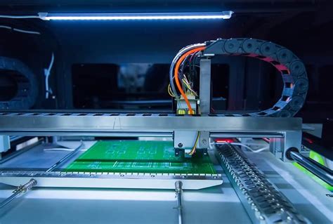
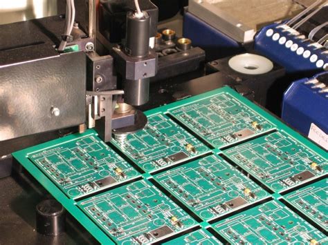
Modern PCB assembly processes leverage automation to drastically reduce prototyping cycles, enabling engineers to transition from design validation to functional testing in days rather than weeks. By integrating advanced pick-and-place systems and AI-driven optical inspection, automated PCBA workflows eliminate manual errors while maintaining micron-level accuracy. These systems synchronize with computer-aided design (CAD) software, automatically translating schematics into machine-readable instructions for component placement, soldering, and testing.
The adoption of robotic soldering arms and reflow ovens ensures consistent thermal profiles across batches, critical for high-density boards with fine-pitch components. Real-time analytics further refine process parameters, identifying potential defects before physical prototypes are built. This shift not only accelerates iteration speeds but also reduces material waste by up to 30%, aligning with lean manufacturing principles.
For startups and R&D teams, cloud-connected PCB assembly platforms offer instant access to automated production lines, bypassing traditional tooling delays. Engineers can upload designs, select materials, and receive assembled prototypes within 72 hours—a paradigm shift that compresses development timelines and accelerates market readiness for next-generation electronics.
Online PCB Solutions Revolutionizing Electronics
The integration of PCB assembly services into digital platforms has transformed how electronics are designed and manufactured. By leveraging cloud-based PCBA workflows, engineers now access real-time collaboration tools and automated design validation systems, reducing iteration cycles by up to 40%. Platforms offering online PCB assembly enable seamless transitions from schematic design to production-ready files, with features like instant quotation engines and material inventory tracking.
A key advantage lies in the accessibility of advanced manufacturing capabilities. For instance, high-precision relay control modules can now be prototyped and ordered through centralized dashboards, bypassing traditional supply chain delays. Below is a comparison of traditional vs. online PCBA workflows:
| Aspect | Traditional Workflow | Online Workflow |
|---|---|---|
| Quotation Time | 2-5 business days | <1 hour |
| Design Feedback | Manual review | AI-driven analysis |
| Component Sourcing | Vendor-dependent | Global inventory APIs |
These platforms also incorporate predictive analytics to flag potential manufacturing issues, such as solder joint reliability or thermal mismatches, before production begins. By digitizing PCB assembly, businesses achieve faster time-to-market while maintaining compliance with industry standards like IPC-A-610. This shift toward connected manufacturing ecosystems underscores the growing role of online PCBA solutions in driving innovation across consumer electronics, IoT, and industrial automation sectors.
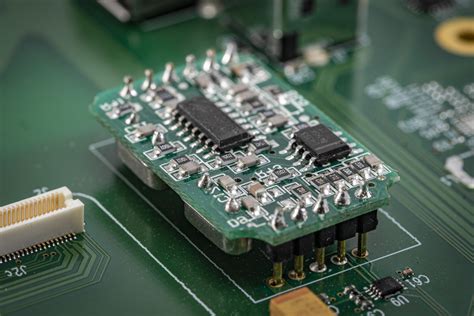
Precision Soldering in Automated PCB Processes
Modern PCB assembly relies on advanced automation to achieve micron-level accuracy in soldering, a critical factor for ensuring reliable electronic connections. Automated PCBA systems employ robotic arms equipped with precision nozzles and vision-guided alignment, enabling consistent application of solder paste across complex circuit layouts. These systems mitigate human error by maintaining strict temperature controls during reflow soldering, ensuring optimal bonding between components and substrates.
The integration of machine learning algorithms further refines soldering quality, analyzing real-time thermal imaging data to adjust parameters like solder volume and placement speed. This adaptive approach is particularly valuable for high-density designs, where even minor deviations can compromise functionality. Additionally, automated optical inspection (AOI) tools verify solder joint integrity post-assembly, flagging defects such as bridging or cold joints for immediate correction.
By combining PCB assembly automation with cloud-based process monitoring, manufacturers achieve traceability and rapid iteration. For instance, surface-mount technology (SMT) lines now synchronize with digital twin models, allowing engineers to simulate and optimize soldering workflows before physical production. This seamless coordination between hardware and software not only accelerates time-to-market but also reduces material waste—a key advantage in scaling PCBA for mass production. As industries demand smaller, faster electronics, precision soldering remains the backbone of reliable, high-performance device manufacturing.

Streamlining Mass Production With Digital Assembly
Digital transformation in PCB assembly has redefined scalability for electronics manufacturers transitioning from prototyping to high-volume production. By integrating smart manufacturing platforms, PCBA providers now leverage automated optical inspection (AOI) systems and digital twin simulations to optimize assembly lines before physical deployment. These tools enable real-time monitoring of solder paste application, component placement accuracy, and thermal profiling—critical factors for maintaining sub-50ppm defect rates in mass production.
Cloud-based PCB assembly platforms further enhance efficiency by synchronizing design files, material inventories, and machine calibration data across global facilities. This digital thread minimizes manual interventions, reducing setup times by 40–60% compared to traditional workflows. For instance, AI-driven demand forecasting adjusts production schedules dynamically, aligning PCBA output with market needs while preventing overstocking.
The shift toward Industry 4.0 standards also introduces modular production cells, where robotic arms and conveyor systems adapt to varying batch sizes without retooling delays. Such flexibility allows manufacturers to scale from 1,000 to 100,000 units per month while maintaining ±0.1mm placement tolerances. As a result, brands accelerate time-to-market without compromising the reliability required for consumer electronics, automotive systems, or industrial IoT devices—key sectors driving demand for digital PCB assembly solutions.
How Automated PCB Assembly Cuts Lead Times
Automated PCB assembly systems eliminate bottlenecks in traditional manufacturing by integrating advanced robotics, AI-driven workflows, and real-time data analytics. Unlike manual processes, which require hours of component placement and solder verification, automated PCBA lines complete these tasks in minutes. For example, high-speed pick-and-place machines position surface-mount devices (SMDs) with micron-level accuracy, reducing alignment errors by up to 98% compared to human operators. This precision minimizes post-assembly rework, shaving days off production schedules.
Cloud-based platforms further compress timelines by enabling seamless collaboration between design teams and manufacturers. Engineers can upload design files digitally, triggering instant material checks and automated procurement of components through connected supplier networks. A recent study highlights that such integrations cut material sourcing delays by 40%, ensuring parts arrive just-in-time for assembly. Additionally, automated optical inspection (AOI) systems scan boards at speeds exceeding 500 components per minute, flagging defects early and preventing costly mid-production halts.
By streamlining workflows from design to delivery, automated PCB assembly transforms what once took weeks into a matter of days—critical for industries racing to meet tight product launch deadlines.
Benefits of Cloud-Based PCB Manufacturing
Cloud-based PCB assembly platforms are transforming electronics production by enabling seamless collaboration between designers, engineers, and manufacturers. Unlike traditional workflows that rely on fragmented communication, these digital solutions centralize project management, allowing stakeholders to review design files, track PCBA progress, and approve changes in real time. This connectivity reduces errors caused by version mismatches and accelerates decision-making cycles by up to 40%, according to industry studies.
A key advantage lies in scalability: cloud systems dynamically adjust computing resources to handle complex simulations or large-scale PCB assembly orders without requiring physical infrastructure upgrades. Manufacturers can also leverage predictive analytics to optimize material procurement and machine utilization, minimizing waste and downtime. For instance, automated alerts for component shortages or thermal irregularities during soldering phases ensure proactive adjustments.
Furthermore, cloud platforms support remote monitoring of PCBA production lines, granting clients visibility into quality control metrics like solder joint integrity or component placement accuracy. This transparency builds trust while aligning with emerging trends in smart manufacturing, where data-driven insights refine process efficiency. By eliminating geographical barriers, cloud-based systems empower startups and enterprises alike to scale production globally while maintaining consistent standards.
Accelerating Product Launches Through Automation
The integration of automated PCB assembly systems into digital manufacturing workflows has become a cornerstone for accelerating time-to-market in electronics development. By leveraging PCBA processes enhanced by robotics and AI-driven quality control, manufacturers can reduce manual intervention while maintaining sub-micron precision in component placement. This automation directly addresses critical bottlenecks in product launch cycles, particularly during design validation and functional testing phases.
Cloud-based platforms now enable real-time collaboration between engineering teams and PCB assembly service providers, allowing rapid iterations without physical prototyping delays. Advanced systems automatically detect soldering defects or component mismatches, slashing rework rates by over 40% in some cases. For mass production, synchronized PCBA lines equipped with adaptive feeders and vision systems achieve first-pass yield rates exceeding 99%, ensuring scale-up readiness within days rather than weeks.
The shift toward smart factory ecosystems further amplifies these benefits, with IoT-enabled PCB assembly machines providing predictive maintenance alerts and yield analytics. This closed-loop automation not only compresses lead times but creates a data-driven foundation for continuous process optimization – a decisive advantage in industries where being first to market translates to capturing 30-50% of category revenue.
Smart Factories Reshaping PCB Assembly Online
The integration of smart factories into PCB assembly processes marks a paradigm shift in electronics manufacturing. By leveraging IoT-enabled machinery and AI-driven analytics, these advanced production hubs optimize PCBA workflows in real time. Sensors embedded in assembly lines monitor solder paste application, component placement accuracy, and thermal profiles, automatically adjusting parameters to maintain six-sigma quality levels. This closed-loop system reduces human intervention while ensuring precision soldering and minimizing rework rates—critical for high-volume orders.
Cloud-connected PCB assembly online platforms further enhance smart factory efficiency. Manufacturers collaborate with global partners through digital twins, simulating production runs to identify bottlenecks before physical assembly begins. For instance, predictive maintenance algorithms preempt equipment downtime, ensuring uninterrupted streamlined mass production. Such systems also synchronize with supply chain databases, automatically reordering components when inventory thresholds dip—a feature particularly valuable for just-in-time manufacturing models.
As smart factories evolve, they increasingly support hybrid workflows where automated PCB assembly coexists with legacy systems. This adaptability allows manufacturers to scale operations without overhauling existing infrastructure, making advanced PCBA technologies accessible even to mid-sized enterprises. By merging industrial automation with cloud computing, these facilities are redefining how electronics reach markets—faster, leaner, and with unprecedented consistency.
Conclusion
The integration of automated PCB assembly into digital workflows marks a transformative shift in electronics manufacturing. By leveraging cloud-based PCBA platforms, businesses can now achieve unprecedented speed and accuracy, bridging the gap between prototyping and full-scale production. These systems not only optimize precision soldering but also enable real-time collaboration across global teams, reducing errors and material waste. As the industry evolves, smart factories are becoming central to scalable operations, where machine learning and IoT-driven analytics refine every stage of PCB assembly online.
For innovators, this means faster iterations, tighter quality control, and the ability to respond dynamically to market demands. The shift toward digitized PCBA processes ensures that even complex designs transition seamlessly from concept to consumer, slashing lead times by up to 60% in some cases. Ultimately, the convergence of automation and digital connectivity is redefining competitiveness, empowering manufacturers to deliver cutting-edge electronics with agility and reliability—key drivers in an era where technological obsolescence looms ever closer.
Frequently Asked Questions
How does automated PCB assembly differ from traditional methods?
Automated PCBA leverages robotic systems and AI-driven inspection to enhance accuracy and speed, reducing human error in tasks like component placement and soldering.
Can online PCB assembly platforms handle complex designs?
Yes, advanced platforms support multi-layer boards, high-density interconnects, and mixed-technology components, ensuring compatibility with cutting-edge electronics.
What role does precision soldering play in automated PCBA?
Automated soldering systems maintain consistent temperatures and solder flow, critical for miniaturized components and high-reliability applications like medical or aerospace devices.
How does cloud-based PCB assembly improve scalability?
Digital platforms enable real-time collaboration, inventory tracking, and demand forecasting, allowing manufacturers to scale production without delays.
Are automated PCBA processes cost-effective for small batches?
Modern systems optimize material usage and setup times, making low-volume runs economical while maintaining the same quality as mass production.
What safeguards ensure quality in online PCB assembly services?
Automated optical inspection (AOI) and electrical testing protocols validate every board, ensuring compliance with industry standards.
Explore Advanced Solutions for Your Projects
Please click here to discover tailored PCB assembly services designed to accelerate your product development cycle.