Balancing HDI PCB Cost and Performance in Modern Electronics
Key Takeaways
When optimizing HDI PCB cost-performance balance, understanding the interplay between design choices and PCB manufacturing cost is critical. You’ll need to evaluate how design complexity—such as microvia density or layer count—affects both performance and expenses. For instance, while advanced via-in-pad techniques improve signal integrity, they may require specialized processes that raise PCB manufacturing overhead. Partnering with experienced PCB manufacturing companies can help identify cost-efficient alternatives without compromising quality.
Tip: Always request a Design for Manufacturability (DFM) review early in the process—this helps catch potential cost drivers like excessive laser drills or non-standard materials.
Material selection also plays a pivotal role. High-speed laminates might enhance performance but could inflate your PCB manufacturing business budget. Instead, consider mid-tier materials that meet your application’s thermal and electrical needs while staying cost-effective. Additionally, consolidating layers through smart stackup design reduces material waste and simplifies assembly.
Remember, balancing high-density applications with budget constraints often involves trade-offs. For example, reducing blind/buried via counts might lower costs but could limit routing flexibility. Explore advanced HDI strategies to refine this equilibrium further. By aligning your design priorities with PCB manufacturing capabilities, you can achieve optimal performance without overspending.
HDI PCB Cost-Performance Optimization Strategies
To achieve optimal balance in HDI PCB designs, you must strategically navigate competing priorities between performance demands and pcb manufacturing cost. Start by evaluating design complexity—every additional microvia or stacked layer increases production challenges, directly impacting your pcb manufacturing business budget. Work closely with pcb manufacturing companies during the prototyping phase to identify areas where simplification can reduce expenses without compromising signal integrity.
Another critical aspect is via-in-pad utilization. While this technique enhances circuit density, improper implementation raises reliability risks and rework costs. Advanced pcb manufacturing partners often recommend hybrid via structures or staggered drilling to maintain performance while controlling pcb manufacturing cost.
| Design Factor | Cost Impact | Performance Benefit |
|---|---|---|
| Microvia Stacking | High | Superior Signal Integrity |
| Low-loss Materials | Moderate | High-frequency Efficiency |
| Sequential Lamination | Variable | Layer Flexibility |
Material selection further influences this equilibrium. High-speed laminates like Megtron 6 deliver exceptional electrical properties but may strain budgets, whereas mid-tier alternatives balance pcb manufacturing cost and functionality for many applications. Finally, optimize layer stackups by aligning dielectric thickness and copper weights with actual performance requirements—over-engineering here unnecessarily inflates expenses. By prioritizing collaboration with experienced pcb manufacturing companies, you ensure technical specifications align with fiscal realities, achieving cost-effective high-density solutions.

Balancing Design Complexity and Manufacturing Expenses
When designing HDI PCBs, you face a critical challenge: aligning advanced features with PCB manufacturing cost efficiency. Higher design complexity—such as increased layer counts, blind/buried vias, or tighter trace spacing—directly impacts PCB manufacturing business expenses. While these features enhance performance, they require specialized equipment and extended production time, driving up costs. To optimize this balance, prioritize functionality-critical elements and simplify non-essential areas. For example, consolidating via types or reducing unnecessary signal layers can lower PCB manufacturing overhead without compromising performance.
Collaborating early with PCB manufacturing companies helps identify cost-saving opportunities. Many providers offer design-for-manufacturability (DFM) checks to flag overly complex features that inflate budgets. Techniques like via-in-pad or staggered microvias, when applied strategically, reduce layer counts and drilling cycles. Material selection also plays a role—using mid-range laminates instead of premium options for non-critical layers can trim PCB manufacturing cost while maintaining reliability. By systematically evaluating trade-offs, you ensure high-density designs meet both technical and financial targets.
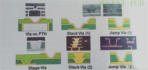
Via-in-Pad Efficiency for Cost-Effective HDI Designs
When optimizing HDI PCB designs, via-in-pad technology plays a critical role in balancing performance and pcb manufacturing cost. By embedding vias directly into component pads, you reduce layer count and signal path lengths, which enhances electrical performance while shrinking board size. However, this approach demands precise engineering to avoid reliability issues like thermal stress or solder wicking—factors that can escalate expenses if not managed properly.
Pcb manufacturing companies often recommend laser-drilled microvias for via-in-pad applications due to their superior accuracy and compatibility with high-density layouts. While laser drilling increases upfront pcb manufacturing costs, it minimizes material waste and reduces the need for additional lamination cycles, ultimately lowering overall project expenses. For instance, consolidating via structures through efficient design software can cut fabrication steps by up to 30%, directly impacting your pcb manufacturing business budget.
To maximize cost efficiency, collaborate with fabricators early to align design choices with their process capabilities. Prioritize via fill materials that match your thermal and mechanical requirements without over-specifying. This balance ensures reliability in high-frequency or high-temperature environments while avoiding unnecessary pcb manufacturing complexity. By strategically implementing via-in-pad techniques, you achieve tighter interconnects without compromising affordability—a key consideration for competitive HDI PCB projects.
Material Selection Impact on HDI PCB Budgets
When optimizing HDI PCB designs, your choice of materials directly influences both performance and pcb manufacturing cost. High-frequency laminates like Rogers or Teflon offer superior signal integrity but can increase expenses by 30-50% compared to standard FR-4. For cost-sensitive projects, hybrid stackups—combining premium materials in critical layers with economical substrates—help balance electrical requirements and pcb manufacturing business budgets.
Thinner dielectrics enable tighter layer spacing, reducing overall board thickness, but require advanced processing tools that some pcb manufacturing companies may charge extra for. Similarly, low-loss prepregs minimize signal attenuation in high-speed applications, though their thermal stability demands precise lamination controls. You’ll need to evaluate whether these features align with your application’s needs or if standard alternatives suffice.
Supplier partnerships also play a role: bulk purchasing of specialized materials or leveraging a manufacturer’s existing inventory can lower per-unit costs. Always request detailed breakdowns of material-related charges during pcb manufacturing quotes to identify areas for negotiation. By aligning material properties with functional requirements, you avoid over-engineering while maintaining reliability—a key strategy for managing pcb manufacturing cost without compromising HDI performance.
High-Density Applications: Cost Drivers and Solutions
When designing high-density interconnect (HDI) PCBs for advanced electronics, you’ll face unique cost challenges tied to tighter tolerances and intricate layouts. Key drivers like microvia density, blind/buried via configurations, and layer count directly influence PCB manufacturing cost, especially in applications requiring signal integrity for 5G or IoT devices. For instance, via-in-pad techniques reduce space but demand precision drilling and plating, adding expenses. To balance this, work closely with PCB manufacturing companies to optimize designs for their production capabilities—simplifying via structures or using staggered instead of stacked microvias can lower fabrication complexity without sacrificing performance.
Material selection also plays a critical role. High-frequency laminates or low-loss dielectrics might be necessary for performance but can inflate PCB manufacturing business budgets. Consider hybrid stackups: pairing premium materials only in critical layers with standard FR-4 elsewhere. Additionally, leveraging advanced DFM (design for manufacturability) tools helps identify cost traps early, such as unnecessary laser drills or excessive solder mask openings. By aligning your design choices with PCB manufacturing realities, you maintain functionality while avoiding over-engineering—a strategic approach to managing both technical and financial demands in high-density projects.
Minimizing Expenses in Advanced PCB Layer Stackups
When designing advanced layer stackups for PCB manufacturing, balancing performance requirements with PCB manufacturing cost starts with understanding how layer count and material choices impact budgets. While high-layer-count designs enable complex routing, they directly increase material usage and production time. You can optimize this by collaborating with experienced PCB manufacturing companies to identify the minimum number of layers needed for signal integrity, avoiding over-engineering. For instance, using via-in-pad techniques reduces the need for additional layers by maximizing interconnect density within existing ones.
Material selection also plays a critical role. High-speed substrates like low-loss laminates may be necessary for specific applications, but standard FR-4 alternatives often suffice for cost-sensitive projects. Prioritize materials that meet electrical specs without exceeding performance thresholds—this requires clear communication with your PCB manufacturing business partner early in the design phase.
Additionally, consider sequential lamination strategies to group critical layers, minimizing lamination cycles and associated costs. Advanced simulation tools help validate stackup configurations before production, reducing trial-and-error expenses. By aligning design decisions with PCB manufacturing capabilities—such as standard panel sizes and preferred via technologies—you avoid costly customizations. Every adjustment should aim to simplify fabrication while maintaining functionality, ensuring your high-density design stays within budget without compromising reliability.
Optimizing HDI Manufacturing for Budget Constraints
When balancing PCB manufacturing expenses for high-density interconnect designs, you need to prioritize processes that reduce PCB manufacturing cost without compromising reliability. Start by collaborating with experienced PCB manufacturing companies to identify yield-enhancing techniques—such as optimized laser drilling parameters or advanced registration systems—that minimize material waste. For instance, consolidating microvia layers or using hybrid stackups can lower PCB manufacturing business overheads while maintaining signal integrity.
Transitioning from prototype to volume production requires careful planning. Standardizing panel utilization and negotiating bulk material pricing with suppliers often shaves 12–18% off per-unit costs. Additionally, adopting design-for-manufacturability (DFM) guidelines tailored to your PCB manufacturing partner’s capabilities prevents costly redesigns. For example, avoiding ultra-fine traces below 3 mil unless absolutely necessary reduces scrap rates.
Finally, evaluate whether value-added services like automated optical inspection (AOI) or sequential lamination align with your budget. While these steps add upfront PCB manufacturing cost, they mitigate risks of field failures—a critical consideration for mission-critical applications. By aligning your design choices with scalable production workflows, you ensure cost predictability without sacrificing the performance demands of modern electronics.
Evaluating Trade-Offs Between Performance and PCB Costs
When optimizing HDI PCB designs, balancing technical requirements with PCB manufacturing cost demands careful analysis. Higher layer counts, microvias, and advanced materials directly influence performance but escalate expenses. For example, while via-in-pad techniques reduce signal loss, they require specialized drilling and plating processes, increasing production complexity. To manage budgets, you must prioritize features that align with your application’s core needs—avoid overengineering non-critical sections.
Collaborating with experienced PCB manufacturing companies helps identify cost-saving opportunities without sacrificing reliability. For instance, opting for standard FR-4 substrates instead of high-frequency laminars might suffice for moderate-speed applications, trimming PCB manufacturing business overheads. However, high-density designs for aerospace or medical devices often justify premium material costs to meet stringent performance standards.
Analyzing PCB manufacturing workflows—like panel utilization rates or testing protocols—can further reduce waste. Some manufacturers offer design-for-manufacturability (DFM) reviews to spot inefficiencies early. Remember: a 20–30% cost increase from advanced features may be unavoidable in cutting-edge applications, but strategic compromises in layer stackups or via types can mitigate expenses. The key lies in transparent communication with your fabrication partner to align technical ambitions with fiscal realities.
Conclusion
Achieving the optimal balance between HDI PCB cost and performance ultimately depends on strategic decision-making across design and production stages. By prioritizing via-in-pad efficiency and minimizing layer stackup complexity, you can reduce PCB manufacturing cost without compromising signal integrity. Collaborating with experienced PCB manufacturing companies ensures access to advanced processes that streamline high-density designs while controlling expenses. Material selection remains critical—opting for mid-range substrates that meet thermal and mechanical demands often provides the best cost-to-performance ratio for most applications. When evaluating PCB manufacturing business partnerships, consider their expertise in handling microvias and sequential lamination, as these capabilities directly impact yield rates and long-term reliability. Remember that cost optimization isn’t about cutting corners but making informed trade-offs between technical requirements and budget constraints. As HDI technologies evolve, maintaining this equilibrium will require continuous dialogue between design teams and manufacturers to align innovation with financial feasibility.
FAQs
How does design complexity affect HDI PCB manufacturing cost?
Increased layer counts and microvia density directly impact PCB manufacturing expenses due to specialized equipment requirements. You can mitigate costs by collaborating with PCB manufacturing companies that offer design-for-manufacturability (DFM) analysis to optimize layouts without compromising functionality.
What makes via-in-pad techniques cost-effective?
Embedding vias within pads reduces layer transitions and improves signal integrity, lowering material waste and assembly time. Partnering with experienced PCB manufacturing business providers ensures precise implementation, avoiding rework costs associated with misaligned features.
How does material selection influence HDI PCB budgets?
High-frequency laminates or low-loss dielectrics increase PCB manufacturing cost, but alternatives like FR-4 hybrids may suffice for non-critical applications. Discuss performance requirements with your manufacturer to balance thermal stability and budget constraints.
What are key cost drivers in high-density applications?
Miniaturization demands advanced processes like laser drilling and sequential lamination, which escalate expenses. Optimize designs by limiting blind/buried via ratios and leveraging panelization strategies offered by PCB manufacturing specialists.
Can you reduce costs without sacrificing reliability?
Yes. Standardizing finishes (e.g., ENIG over gold plating) and opting for bulk material purchases often lowers PCB manufacturing cost. Many PCB manufacturing companies provide tiered pricing for prototype-to-production scaling.
How do you evaluate performance vs. cost trade-offs?
Prioritize critical features like impedance control or thermal management while simplifying non-essential layers. Request detailed cost breakdowns from PCB manufacturing business partners to identify areas for compromise.
Ready to Optimize Your HDI PCB Project?
For tailored solutions that balance performance and PCB manufacturing cost, please click here to consult experts specializing in high-density designs.


