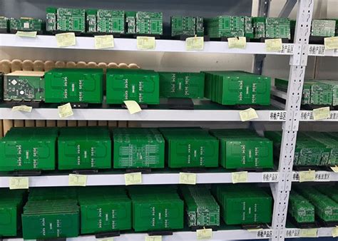
Bare PCB Board: The Foundation of Modern Electronics
Introduction
In the realm of modern electronics, the Printed Circuit Board (PCB) is an indispensable component that serves as the backbone of virtually every electronic device. Among the various types of PCBs, the bare PCB board, also known as an unpopulated or blank PCB, holds a unique and critical position. This article delves into the intricacies of bare PCB boards, exploring their definition, manufacturing process, types, applications, advantages, and challenges.
1. Definition of Bare PCB Board
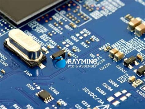
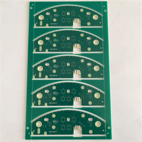
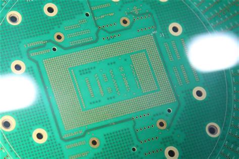
A bare PCB board is a flat, rigid, or flexible substrate made from insulating materials, such as fiberglass, epoxy resin, or polyimide, with conductive pathways etched or printed onto its surface. These pathways, typically made of copper, form the electrical connections between various electronic components. Unlike assembled PCBs, bare PCBs do not have any components mounted on them; they are essentially the “skeleton” upon which the electronic components are later attached.
2. Manufacturing Process of Bare PCB Boards
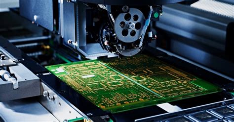
The manufacturing of bare PCB boards is a multi-step process that requires precision and attention to detail. The key steps involved are:
2.1. Design and Layout
The process begins with the design of the PCB layout using specialized software. Engineers create a schematic diagram that outlines the electrical connections and component placements. This design is then translated into a physical layout, specifying the exact locations of the conductive pathways, vias, and pads.
2.2. Material Selection
The choice of substrate material is crucial and depends on the intended application of the PCB. Common materials include FR-4 (a composite of fiberglass and epoxy), polyimide for flexible PCBs, and metal-core substrates for high-power applications.
2.3. Printing the Circuit Pattern
The circuit pattern is transferred onto the substrate using a photolithographic process. A photosensitive layer, called the photoresist, is applied to the copper-clad substrate. The desired circuit pattern is then exposed to ultraviolet light through a photomask, hardening the exposed areas of the photoresist.
2.4. Etching
The unexposed areas of the photoresist are removed, exposing the underlying copper. The board is then immersed in an etching solution, which removes the exposed copper, leaving behind the desired conductive pathways.
2.5. Drilling and Plating
Holes are drilled into the board to accommodate through-hole components and vias. These holes are then plated with copper to establish electrical connections between different layers of the PCB.
2.6. Solder Mask Application
A solder mask is applied to the board to protect the copper traces from oxidation and prevent solder bridges during component assembly. The solder mask is typically green, but other colors are also available.
2.7. Surface Finish
The final step involves applying a surface finish to the exposed copper pads to enhance solderability and protect against corrosion. Common surface finishes include HASL (Hot Air Solder Leveling), ENIG (Electroless Nickel Immersion Gold), and OSP (Organic Solderability Preservative).
3. Types of Bare PCB Boards
Bare PCB boards come in various types, each suited to specific applications and requirements. The main types include:
3.1. Single-Sided PCBs
These PCBs have conductive pathways on only one side of the substrate. They are the simplest and most cost-effective type, suitable for basic electronic devices.
3.2. Double-Sided PCBs
Double-sided PCBs have conductive pathways on both sides of the substrate, allowing for more complex circuits and higher component density. They are commonly used in consumer electronics and industrial controls.
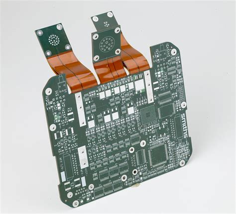
3.3. Multi-Layer PCBs
Multi-layer PCBs consist of three or more layers of conductive pathways, separated by insulating layers. They are used in advanced applications such as telecommunications, medical devices, and aerospace systems, where high circuit complexity and signal integrity are required.
3.4. Flexible PCBs
Flexible PCBs are made from flexible substrates, such as polyimide, allowing them to bend and conform to different shapes. They are used in applications where space and weight are critical, such as wearable devices and flexible displays.
3.5. Rigid-Flex PCBs
Rigid-flex PCBs combine the benefits of rigid and flexible PCBs, offering both structural stability and flexibility. They are used in complex applications like military and medical equipment, where reliability and space optimization are paramount.
4. Applications of Bare PCB Boards
Bare PCB boards are the foundation of a wide range of electronic devices and systems. Some of the key applications include:
4.1. Consumer Electronics
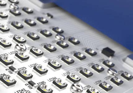
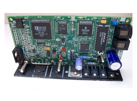
Bare PCBs are used in smartphones, tablets, laptops, and home appliances, providing the necessary electrical connections for these devices to function.
4.2. Automotive Industry
In the automotive sector, bare PCBs are used in engine control units, infotainment systems, and advanced driver-assistance systems (ADAS), contributing to the safety and performance of modern vehicles.
4.3. Industrial Automation
Bare PCBs are integral to industrial automation systems, including programmable logic controllers (PLCs), sensors, and robotics, enabling efficient and precise control of manufacturing processes.
4.4. Medical Devices
In the medical field, bare PCBs are used in diagnostic equipment, imaging systems, and implantable devices, where reliability and precision are critical.
4.5. Aerospace and Defense
Bare PCBs are employed in avionics, communication systems, and radar systems in the aerospace and defense industries, where they must withstand extreme conditions and provide high performance.
5. Advantages of Bare PCB Boards
Bare PCB boards offer several advantages that make them the preferred choice for electronic circuit design:
5.1. Compact Design
PCBs allow for the miniaturization of electronic devices by providing a compact and organized platform for component placement and interconnection.
5.2. Reliability
The use of PCBs reduces the risk of loose connections and short circuits, enhancing the reliability and longevity of electronic devices.
5.3. Ease of Assembly
Bare PCBs simplify the assembly process, as components can be easily mounted and soldered onto the board using automated machinery.
5.4. Cost-Effectiveness
Mass production of bare PCBs is cost-effective, making them an economical solution for large-scale manufacturing.
5.5. Customizability
PCBs can be customized to meet specific design requirements, allowing for the creation of tailored solutions for different applications.
6. Challenges in Bare PCB Manufacturing
Despite their numerous advantages, the manufacturing of bare PCB boards is not without challenges:
6.1. Complexity
As electronic devices become more advanced, the complexity of PCB designs increases, requiring more layers, finer traces, and tighter tolerances.
6.2. Material Limitations
The choice of substrate material can impact the performance of the PCB, particularly in high-frequency or high-temperature applications.
6.3. Environmental Concerns
The manufacturing process involves the use of chemicals and generates waste, raising environmental concerns and necessitating the adoption of sustainable practices.
6.4. Quality Control
Ensuring the quality and reliability of bare PCBs requires rigorous testing and inspection, which can be time-consuming and costly.
6.5. Miniaturization
The trend towards smaller and more compact devices poses challenges in terms of component placement, heat dissipation, and signal integrity.
7. Future Trends in Bare PCB Technology
The future of bare PCB technology is shaped by ongoing advancements in materials, manufacturing processes, and design techniques. Some of the key trends include:
7.1. High-Density Interconnect (HDI) PCBs
HDI PCBs feature finer traces and smaller vias, enabling higher component density and improved signal integrity. They are increasingly used in smartphones, tablets, and other compact devices.
7.2. Flexible and Stretchable PCBs
The development of flexible and stretchable PCBs is opening up new possibilities for wearable devices, medical implants, and other applications where traditional rigid PCBs are not suitable.
7.3. Embedded Components
Embedding passive and active components within the PCB substrate is gaining traction, offering benefits such as reduced size, improved performance, and enhanced reliability.
7.4. 3D Printing
3D printing technology is being explored for the rapid prototyping and production of PCBs, allowing for greater design flexibility and faster time-to-market.
7.5. Sustainable Manufacturing
The adoption of eco-friendly materials and processes, such as lead-free soldering and recycling of PCB waste, is becoming increasingly important in the PCB industry.
Conclusion
Bare PCB boards are the unsung heroes of modern electronics, providing the essential foundation upon which electronic devices are built. From their intricate manufacturing process to their diverse applications and advantages, bare PCBs play a pivotal role in shaping the technological landscape. As the demand for more advanced and compact electronic devices continues to grow, the evolution of bare PCB technology will remain at the forefront of innovation, driving progress in various industries and enabling the development of cutting-edge solutions. Despite the challenges, the future of bare PCB boards is bright, with emerging trends promising to further enhance their capabilities and expand their applications.