Bare PCB Manufacturing: A Comprehensive Guide to the Process

Key Takeaways
When engaging with bare PCB manufacturing, it is crucial to appreciate its role in the broader context of electronic device production. The process begins with understanding the fundamentals of PCB manufacturing, where each stage contributes to the final product’s functionality and reliability. You’ll find that PCB manufacturing companies often emphasize rigorous design protocols, ensuring that layouts are optimized for performance and efficiency. Moreover, it’s important to assess PCB manufacturing cost, as this factor influences your decision-making when selecting materials and processes. For anyone in the PCB manufacturing business, staying ahead of innovations and adhering to industry standards can significantly improve product quality while minimizing common hurdles faced during production. Exploring these aspects will provide you with valuable insights into how to achieve successful results in your projects, ultimately leading to superior printed circuit boards tailored for a variety of applications. For further information on best practices and updates in this domain, consider visiting Andwin PCB.
Understanding Bare PCB: Definition and Importance
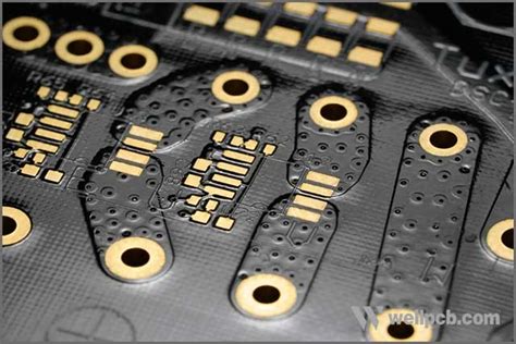
Understanding bare PCBs (Printed Circuit Boards) is essential for anyone involved in the PCB manufacturing industry. A bare PCB typically refers to the basic board without any soldering or components attached — it’s the foundation upon which electronic circuits are built. This initial stage of production is critical because it sets the groundwork for performance, reliability, and functionality in the final product. The importance of bare PCBs lies in their role as a substrate that supports electrical paths; they affect signal integrity and overall system efficiency. When you engage with PCB manufacturing companies, you’ll discover that a thorough understanding of how to design and produce bare PCBs significantly influences the PCB manufacturing cost and enables better decision-making regarding materials and processes.
Moreover, investing in a quality PCB manufacturing business that prioritizes effective design processes and material selection can lead to enhanced product durability and performance. An industry-standard bare PCB can significantly reduce failure rates in later production stages, ensuring that your final product operates as intended across various applications. As competitive pressures mount within global markets, staying adept in every aspect of bare PCB production is not just advantageous — it’s essential for maintaining market relevance.
"The journey from concept to creation begins with a solid understanding of your base materials."
The Design Process: Creating an Effective PCB Layout
In the realm of bare PCB manufacturing, the design process is crucial for the successful realization of your project. It begins with conceptualizing the purpose of your printed circuit board. You must consider factors such as the physical dimensions, electronic specifications, and functional requirements that align with industry standards. To create an effective PCB layout, utilizing specialized software is vital. These tools allow you to simulate and optimize component placement, ensuring that signals travel efficiently and reducing potential interference.
When designing your PCB, it’s essential to adhere to design rules established by leading PCB manufacturing companies. These rules help maintain proper spacing between traces and prevent issues like short circuits or signal degradation. You might want to create a preliminary schematic before moving onto the layout phase, which helps clarify how components interconnect.
In terms of costs, it’s beneficial to keep an eye on the PCB manufacturing cost during this phase. By optimizing your layout for fewer layers or minimizing intricate designs without compromising functionality, you can significantly lower expenses. Designing a well-thought-out layout not only enhances performance but also impacts your overall PCB manufacturing business efficiency.
Moreover, consider using tables or diagrams within your design documents to illustrate component positions clearly; this adds value when presenting your design to stakeholders or team members for feedback. By focusing on these aspects during the design process, you’re setting a solid foundation for quality fabrication and performance in your bare PCBs.
| Design Consideration | Description |
|---|---|
| Component Placement | Strategic positioning to minimize trace lengths |
| Layer Count | Reducing layers can lower costs |
| Trace Width | Ensuring adequate thickness for current handling |
| Ground Plane | Enhancing electromagnetic compatibility |
By following best practices in this critical stage of bare PCB manufacturing, you can ensure a smoother transition into subsequent phases such as fabrication and testing.
Materials Used in Bare PCB Manufacturing
In the realm of bare PCB manufacturing, the selection of materials is a critical step that directly influences the performance and reliability of the final product. The most commonly used substrate material is fiberglass-reinforced epoxy resin, often referred to as FR-4, due to its excellent electrical insulation properties and mechanical strength. When you embark on your journey in the pcb manufacturing business, carrying knowledge about these materials can help you make informed decisions regarding pcb manufacturing costs.
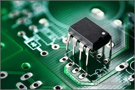
Additionally, you might encounter other substrate materials such as polyimide for high-temperature applications and ceramic materials for specific RF applications. Each material offers unique benefits depending on the intended final use of the circuit board, which can affect your choice of pcb manufacturing companies. Moreover, various conductive materials, such as copper, are used for pathways and connections on the PCB. The thickness and treatment of copper can also impact electrical performance and durability.
Understanding these material choices is essential for ensuring that your PCB meets industry standards and customer expectations. By focusing on quality components from reputable suppliers, you can enhance your production capabilities while minimizing potential issues in assembly or operation down the line. Ultimately, being well-versed in the nuances of material selection will empower you in your pcb manufacturing endeavors and help foster successful project outcomes.
The Fabrication Process: Step-by-Step Guide
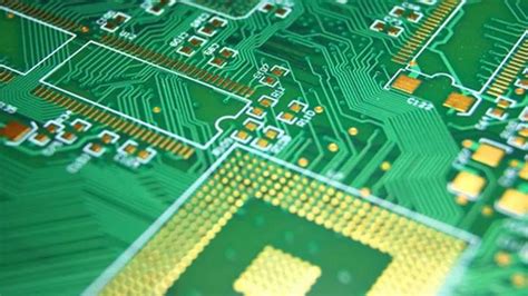
In the realm of bare PCB manufacturing, the fabrication process is a critical phase that encompasses several intricate steps. To begin, you’ll engage in pcb manufacturing by preparing the substrate, which is foundational to the board’s integrity and performance. This substrate, often made from materials like FR-4 (a flame-retardant epoxy resin) or polyimide, must be adequately treated to enhance its bonding capabilities with copper layers. Once your substrate is prepared, pcb manufacturing companies will apply a thin layer of copper to one or both sides of the substrate through processes like electroplating or lamination.
Following this, you will need to etch away unwanted copper using a chemical solution during masking, creating your desired circuit layout. This step ensures that your pcb manufacturing cost remains controlled while maintaining precision in your design. After etching, you’ll drill holes for vias and component placements, which are essential for connectivity in your circuitry.
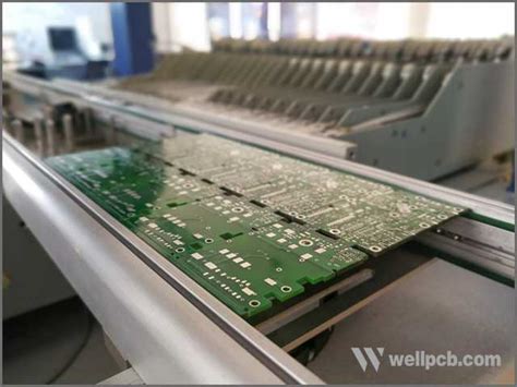
Next comes the application of solder mask—an important layer that protects against short circuits and enhances durability. The final touch involves silkscreen printing, where component designator markings are added for ease of assembly, ultimately contributing to the efficiency of your pcb manufacturing business. Once all these steps are meticulously executed, quality inspections follow to ensure adherence to industry standards before the bare PCBs are ready for shipment or further processing.
Thus, understanding each step in this process not only helps you manage costs effectively but also ensures that high-quality products emerge from your bare PCB manufacturing efforts, ready for their intended applications across various industries.
Quality Control and Industry Standards in PCB Manufacturing
In the realm of PCB manufacturing, ensuring quality is paramount. Quality control encompasses a series of systematic processes that guarantee your bare PCBs meet strict industry standards. This includes thorough testing at various stages of production, from initial design to final assembly, to detect any potential flaws early on. Establishing a robust quality management system helps you navigate the complexities of PCB manufacturing costs, as it reduces waste and rework, ultimately leading to more efficient operations. Understanding the specific requirements set by industry standards, such as IPC-A-600 for acceptability of printed boards, aids you in aligning with the expectations of clients and regulatory bodies. This adherence not only elevates your reputation among PCB manufacturing companies, but also strengthens your PCB manufacturing business by fostering trust and reliability in your products. By focusing on rigorous testing methods—such as Automated Optical Inspection (AOI) and Electrical Testing—you can be confident that each board produced will perform reliably in its intended application, thus reinforcing the significance of quality control throughout the PCB manufacturing process.
Innovations in Bare PCB Technology
As you explore innovations in bare PCB technology, you’ll find that advancements are reshaping the landscape of PCB manufacturing. Today, leading PCB manufacturing companies are pushing the boundaries of design and fabrication, integrating advanced materials and processes to enhance performance and reduce costs. Technologies such as flexible PCBs and high-frequency substrates are becoming increasingly common, ensuring that your PCB solutions meet the demands of modern applications. The use of automation and machine learning in the fabrication process helps optimize production lines, significantly driving down pcb manufacturing costs while improving efficiency. Furthermore, these innovations are critical for helping you navigate the complexities of a competitive pcb manufacturing business, as they enable you to offer more value to your clients. It is vital to stay informed about recent breakthroughs in materials science and design techniques, as these can lead to the development of more reliable and compact circuit boards that cater to industries like telecommunications, automotive, and consumer electronics. By harnessing the latest technologies, you can ensure that your investment in bare PCB development promotes sustainability while meeting rigorous industry standards.
Applications of Bare PCBs Across Industries
Bare PCBs serve an integral role in a variety of industries, offering both versatility and reliability in electronic applications. You’ll find that the demand for bare PCB manufacturing has surged due to advancements in technology and the growing need for efficient electronic solutions. In the automotive industry, for instance, bare PCBs are pivotal in the operation of safety systems, power control units, and infotainment systems, ensuring both performance and safety. The telecommunications sector also heavily relies on bare PCBs, as they form the backbone of devices such as routers and smartphones, providing essential connectivity and data transfer capabilities.
Furthermore, in the medical field, bare PCBs are critical for devices that require high reliability and precision, including diagnostic equipment and wearable health monitors. Their ability to meet stringent regulatory standards is key to ensuring patient safety. In consumer electronics, the lightweight design achieved through effective PCB manufacturing enables innovative gadgets that enhance user experience.
When you consider partnering with PCB manufacturing companies, it’s important to recognize how bare PCBs can reduce overall pcb manufacturing costs while maintaining quality. Companies looking to establish a robust pcb manufacturing business can leverage these factors to ensure they meet industry demands effectively while optimizing their production processes. Overall, the applications of bare PCBs reflect their essential role across various sectors – a testament to their enduring relevance in technology development.
Conclusion
In summary, understanding the nuances of bare PCB manufacturing is essential for anyone involved in the electronics industry. This guide has navigated various steps of the manufacturing process, shedding light on how to achieve high-quality results. It’s crucial to recognize that choosing the right PCB manufacturing companies can significantly influence your project’s success. From material selection to fabrication techniques, every detail impacts the PCB manufacturing cost and, consequently, your bottom line. By applying best practices outlined in this guide, you can optimize your strategies and address common challenges associated with PCB manufacturing. As the landscape continues to evolve with innovations in technology, businesses that adapt will find ample opportunities within the expanding market for bare PCBs. Therefore, equipping yourself with this knowledge not only empowers you but can also enhance your overall success in the PCB manufacturing business.
FAQs
What is bare PCB manufacturing?
Bare PCB manufacturing refers to the process of creating printed circuit boards (PCBs) without any components. It involves several stages, including design, material selection, and fabrication, ensuring the PCBs meet the specific requirements for various electronic applications.
How does the design affect PCB manufacturing?
The design plays a crucial role in pcb manufacturing, as a well-thought-out layout determines the performance and reliability of the final product. Effective design minimizes costs and enhances functionality, which is vital for pcb manufacturing companies striving for high-quality results.
What materials are commonly used in bare PCB manufacturing?
In bare PCB manufacturing, common materials include fiberglass, epoxy resin, cooper foil, and other specialized substances that ensure durability and conductivity. Selecting appropriate materials is essential to control the overall pcb manufacturing cost, impacting both performance and longevity.
What are the common challenges faced during PCB manufacturing?
Challenges such as misalignment, layer adhesion issues, and contamination can arise during production. Companies often focus on quality control measures to mitigate these challenges effectively, ensuring that their pcb manufacturing business can maintain high-quality standards.
How can I reduce costs associated with bare PCB manufacturing?
To lower pcb manufacturing costs, consider optimizing your design for manufacturability, sourcing materials wisely, and selecting reliable manufacturers known for efficiency without compromising quality.
For more detailed insights into PCB manufacturing, please click here: https://www.andwinpcb.com/pcb-manufacturing/


