Basic design methods and principle requirements for printed circuit boards
For an instrument with excellent performance, in addition to selecting high-quality components and reasonable circuits, the correct structural design of the component layout and electrical connection direction of the printed circuit board is a key issue that determines whether the instrument can work reliably. For circuits with the same components and parameters, different results may be produced due to different component layout designs and electrical connection directions. Therefore, it is necessary to consider how to correctly design the structure of the printed circuit board component layout and the correct selection of the wiring direction and the process structure of the overall instrument.
A reasonable process structure can eliminate noise interference caused by improper wiring and facilitate installation, debugging and maintenance in production.
Let’s discuss the above issues. Since there is no strict “definition” and “mode” for excellent “structure”, the following discussion is only for reference. The structure of each instrument must adopt a corresponding structural design plan based on specific requirements (electrical performance, overall structure installation and panel layout requirements, etc.), and compare and modify several feasible design plans repeatedly.
Selection of wiring structure for power supply and ground bus of printed circuit board—-System structure: Analog circuit and digital circuit have many similarities and differences in the design and wiring methods of component layout diagram. In analog circuit, due to the existence of amplifier, the extremely small noise voltage generated by wiring will cause serious distortion of output signal. In digital circuit, TTL noise tolerance is 0.4V~0.6V, CMOS noise tolerance is 0.3~0.45 times of Vcc, so digital circuit has strong anti-interference ability.

Reasonable selection of good power supply and ground bus mode is an important guarantee for reliable operation of instrument. Quite a lot of interference sources are generated through power supply and ground bus, among which the noise interference caused by ground wire is the largest.
Basic principles and requirements for design of printed circuit board diagram
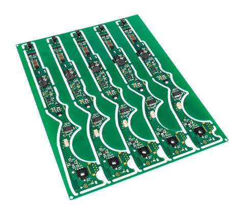
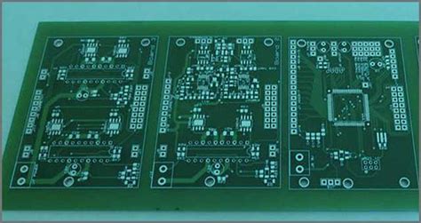
- Design of printed circuit board starts with determining the size of board. The size of printed circuit board is limited by the size of chassis shell, so it is better to fit into the shell. Secondly, the connection method between printed circuit board and external components (mainly potentiometer, socket or other printed circuit board) should be considered. Printed circuit board and external components are generally connected by plastic wire or metal isolation wire. But sometimes it is also designed as a socket. That is: when installing a plug-in printed circuit board in the equipment, a contact position that acts as a socket should be reserved.
For larger components installed on the printed circuit board, metal accessories should be added to fix them to improve vibration and impact resistance.
- Basic methods of wiring diagram design
First, you need to have a complete understanding of the specifications, dimensions, and areas of the selected components and various sockets; make reasonable and careful considerations on the location arrangement of each component, mainly from the perspective of electromagnetic field compatibility, anti-interference, short routing, few crossovers, power supply, ground path and decoupling. After the location of each component is determined, it is the connection of each component, and the relevant pins are connected according to the circuit diagram. There are many ways to complete it. The design of printed circuit diagrams includes computer-aided design and manual design methods.
The most primitive is manual layout.
This is more troublesome and often requires repeated several times before it can be finally completed. This can also be done when there is no other drawing equipment. This manual layout method is also very helpful for those who have just learned printed circuit board designers. Computer-aided drawing. There are many drawing softwares with different functions, but in general, it is convenient to draw and modify, and can be saved, stored and printed.
Next, determine the required size of the printed circuit board, and preliminarily determine the position of each component according to the schematic diagram, and then make the layout more reasonable through continuous adjustments. The wiring arrangement between the components in the printed circuit board is as follows:
(1) No cross circuits are allowed in the printed circuit.
For lines that may cross, you can use “drilling” and “winding” to solve them. That is, let a lead “drill” through the gap under the feet of other resistors, capacitors, and triodes, or “wind” through one end of a lead that may cross. In special cases, if the circuit is very complicated, in order to simplify the design, it is also allowed to use wire jumper to solve the cross circuit problem.
(2) There are two installation methods for components such as resistors, diodes, and tubular capacitors: “vertical” and “horizontal”.
Vertical means that the component body is installed and welded perpendicular to the circuit board, and its advantage is space saving. Horizontal means that the component body is installed and welded parallel to and close to the circuit board, and its advantage is that the mechanical strength of the component installation is good. The component hole spacing on the printed circuit board is different for these two different installation components.
(3) The grounding points of the same level circuit should be as close as possible, and the power filter capacitor of the current level circuit should also be connected to the grounding point of this level.
In particular, the grounding points of the base and emitter of the transistor at this level cannot be too far apart, otherwise the long copper foil between the two grounding points will cause interference and self-excitation. The circuit using such a “one-point grounding method” is more stable and less prone to self-excitation.
(4) The total ground wire must be strictly arranged in the order of high frequency-medium frequency-low frequency from weak current to strong current.
It must not be randomly turned over and over. It is better to have a longer connection between levels, but this rule must be followed. In particular, the grounding arrangement requirements for the frequency conversion head, regeneration head, and frequency modulation head are more stringent. If it is not appropriate, self-excitation will occur and it will not work.
High-frequency circuits such as FM heads often use large-area enclosed ground wires to ensure good shielding effects.
(5) High-current leads (common ground wires, amplifier power leads, etc.) should be as wide as possible to reduce wiring resistance and voltage drop, which can reduce self-excitation caused by parasitic coupling.
(6) High-impedance traces should be as short as possible, and low-impedance traces can be longer, because high-impedance traces are prone to whistling and absorbing signals, causing circuit instability. Power lines, ground wires, base traces without feedback components, emitter leads, etc. are all low-impedance traces. The base traces of the emitter follower and the ground wires of the two channels of the recorder must be separated and each of them is connected to the end of the function. If the two ground wires are connected back and forth, crosstalk is very likely to occur, which reduces the separation.
II. The following points should be noted in the design of printed circuit boards
- Wiring direction: From the welding surface, the arrangement of components should be kept consistent with the schematic diagram as much as possible, and the wiring direction should be consistent with the wiring direction of the circuit diagram. Because various parameters usually need to be tested on the welding surface during the production process, this is convenient for inspection, debugging and maintenance in production (Note: It refers to the premise of meeting the circuit performance and the requirements of the whole machine installation and panel layout).
- The arrangement and distribution of each component should be reasonable and uniform, and strive to meet the process requirements of neatness, beauty and rigorous structure.
- Resistors and diodes can be placed horizontally or vertically:
(1) Horizontal placement: When the number of circuit components is small and the size of the circuit board is large, it is generally better to place them horizontally; for resistors below 1/4W, the distance between the two pads is generally 4/10 inches, and for resistors of 1/2W, the distance between the two pads is generally 5/10 inches; for diodes placed horizontally, 1N400X series rectifiers are generally 3/10 inches; 1N540X series rectifiers are generally 4 to 5/10 inches.
(2) Vertical placement: When the number of circuit components is large and the size of the circuit board is not large, it is generally placed vertically. When placed vertically, the distance between the two pads is generally 1 to 2/10 inches.
4. Potentiometer: Principles of IC socket placement
(1) Potentiometer: It is used to adjust the output voltage in the voltage regulator. Therefore, the potentiometer should be designed so that the output voltage increases when it is adjusted clockwise and decreases when it is adjusted counterclockwise; in the adjustable constant current charger, the potentiometer is used to adjust the charging current. When designing the potentiometer, the current increases when it is adjusted clockwise.
The placement of the potentiometer should meet the requirements of the overall structure installation and panel layout. Therefore, it should be placed on the edge of the board as much as possible with the rotating handle facing outward.
(2) IC socket: When designing a printed circuit board, when using an IC socket, special attention must be paid to whether the positioning groove on the IC socket is placed correctly, and whether the positions of each IC pin are correct. For example, the first pin can only be located at the lower right corner or upper left corner of the IC socket, and close to the positioning groove (from the welding surface).
5.Arrangement of input and output terminals
(1) The distance between the two associated lead terminals should not be too large. Generally, it is more appropriate to be about 2 to 3/10 inches.
(2) The inlet and outlet terminals should be concentrated on 1 to 2 sides as much as possible, and should not be too discrete.
- When designing the wiring diagram, pay attention to the order of pin arrangement and the spacing between component pins should be reasonable.
- Under the premise of ensuring the performance requirements of the circuit, the design should strive to make the routing reasonable, use less external jumpers, and route the wires according to certain charging requirements, and strive to be intuitive, easy to install, high and repair.
- When designing the wiring diagram, try to make the routing as few turns as possible and strive to make the lines simple and clear.
- The width and spacing of the wiring lines should be moderate, and the spacing between the two pads of the capacitor should be as consistent as possible with the spacing of the capacitor lead pins;
- The design should be carried out in a certain order, for example, from left to right and from top to bottom.


