Basic Guidelines for Mixed-Signal PCB Layout Design
1. Introduction
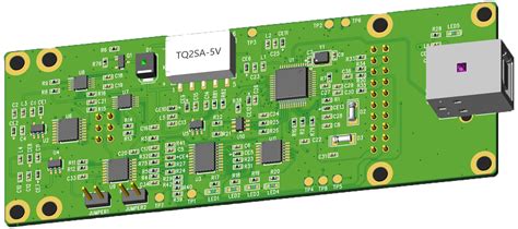
Mixed-signal PCB design involves integrating both analog and digital circuits on the same board. This presents unique challenges due to the differing noise sensitivities and signal integrity requirements of analog and digital components. Proper layout techniques are essential to minimize interference, crosstalk, and signal degradation. This article outlines fundamental guidelines for designing mixed-signal PCBs to ensure optimal performance.
2. Key Challenges in Mixed-Signal PCB Design
The primary challenges in mixed-signal PCB design include:
- Noise Coupling: Digital signals can introduce high-frequency noise into analog circuits.
- Ground Loops: Improper grounding can create return path issues, leading to noise and interference.
- Signal Integrity: Analog signals are sensitive to distortion, while digital signals require clean transitions.
- Power Supply Noise: Switching regulators and digital ICs can inject noise into analog power rails.
To mitigate these issues, careful PCB layout strategies must be followed.
3. Partitioning Analog and Digital Sections
3.1 Physical Separation
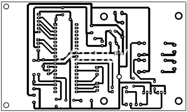
- Separate analog and digital components into distinct regions of the PCB.
- Place sensitive analog circuits (e.g., amplifiers, ADCs, DACs) away from high-speed digital components (e.g., microcontrollers, FPGAs).
- Use a “moat” (a gap with no copper) between analog and digital sections to reduce capacitive coupling.
3.2 Signal Routing Isolation
- Avoid routing digital traces over analog sections and vice versa.
- If crossing is unavoidable, use orthogonal routing (90° angles) to minimize coupling.
- Keep high-speed digital signals (e.g., clocks, data buses) as short as possible and away from analog traces.
4. Grounding Strategies
4.1 Single vs. Split Ground Planes
- Single Ground Plane (Recommended): A unified ground plane with careful partitioning reduces ground loops and provides a low-impedance return path.
- Split Ground Plane (If Necessary): If isolation is critical, split the ground plane but ensure proper stitching (using capacitors or ferrite beads) at a single point to prevent voltage differences.
4.2 Star Grounding for Critical Analog Circuits
- Connect all analog ground returns to a single point (star ground) near the ADC or DAC.
- Avoid ground loops by ensuring that high-current digital return paths do not flow through analog ground regions.
4.3 Proper Use of Ground Pours
- Fill unused PCB areas with ground copper to reduce EMI and improve signal integrity.
- Use via stitching to connect ground planes in multilayer boards, ensuring low impedance.
5. Power Supply Design
5.1 Separate Analog and Digital Power Rails
- Use independent LDO regulators for analog and digital supplies to prevent noise coupling.
- Place ferrite beads or inductors in series with power traces to filter high-frequency noise.
5.2 Decoupling and Bypass Capacitors
- Place 0.1 µF ceramic capacitors close to each IC power pin for high-frequency decoupling.
- Use 10 µF bulk capacitors near power entry points to stabilize supply voltage.
- For sensitive analog circuits, add low-ESR tantalum or polymer capacitors for additional filtering.
6. Signal Routing Best Practices
6.1 Impedance Control for High-Speed Signals
- Match trace impedance (e.g., 50Ω for single-ended, 100Ω for differential pairs) to prevent reflections.
- Use microstrip or stripline configurations for controlled impedance routing.
6.2 Minimizing Crosstalk
- Increase spacing between parallel traces (≥3× trace width).
- Route sensitive analog signals with guard traces (grounded copper on both sides).
6.3 Differential Pair Routing
- Keep differential pairs (e.g., USB, LVDS) tightly coupled with equal length traces to maintain signal integrity.
- Avoid abrupt bends; use curved or 45° angle traces instead of 90° turns.
7. Shielding and EMI Mitigation
7.1 Enclosure and PCB Shielding
- Use metal shields or conductive coatings over sensitive analog circuits.
- Implement grounded copper fences around high-frequency digital sections.
7.2 Filtering and Ferrite Beads
- Add ferrite beads on power and signal lines entering analog zones to suppress high-frequency noise.
- Use common-mode chokes for differential signals to reduce EMI.
8. Thermal Management Considerations
- Place heat-generating digital components (e.g., processors, FPGAs) away from analog circuits.
- Use thermal vias and copper pours to dissipate heat efficiently.
9. Testing and Validation
- Perform frequency-domain analysis (e.g., FFT) to identify noise coupling.
- Use oscilloscope probing to verify signal integrity.
- Conduct EMI/EMC testing to ensure compliance with regulatory standards.
10. Conclusion
Designing mixed-signal PCBs requires careful attention to partitioning, grounding, power distribution, and signal routing. By following these guidelines, engineers can minimize noise, crosstalk, and interference, ensuring reliable operation of both analog and digital circuits. Proper layout techniques, combined with thorough testing, are essential for achieving high-performance mixed-signal designs.

