Best 4 layer pcb stackup
Optimal Signal Integrity in 4 Layer PCB Stackup
When designing a 4-layer printed circuit board (PCB), achieving optimal signal integrity is paramount. Signal integrity refers to the quality and reliability of electrical signals as they travel through the PCB. A well-thought-out stackup can significantly enhance signal integrity, reduce electromagnetic interference (EMI), and improve overall performance. Therefore, understanding the best practices for a best 4-layer PCB stackup is essential for engineers and designers.
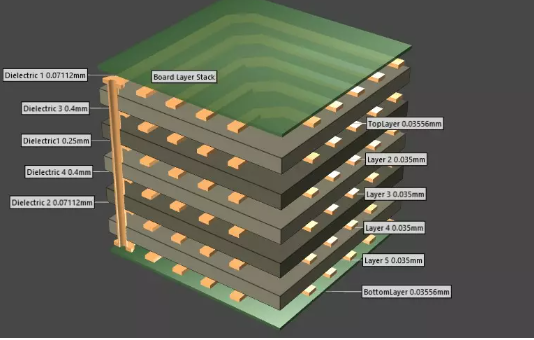
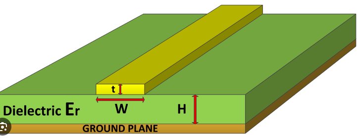
To begin with, a typical 4-layer PCB stackup consists of two signal layers and two planes, usually one for power and one for ground.
The arrangement of these layers plays a crucial role in maintaining signal integrity. A common and effective stackup configuration is: Signal 1, Ground, Power, and Signal 2. This configuration ensures that each signal layer is adjacent to a plane, which helps in minimizing the loop area and reducing EMI.
The placement of the ground plane directly beneath the top signal layer is particularly beneficial.
This proximity allows for a low-impedance return path for high-frequency signals, thereby reducing the risk of signal degradation. Additionally, the ground plane acts as a shield, protecting the signal layer from external noise and interference. Similarly, placing the power plane next to the bottom signal layer provides a stable reference for the signals, further enhancing signal integrity.
Moreover, the separation between the layers is another critical factor.
The dielectric material between the layers should be chosen carefully to ensure the right balance between layer spacing and overall board thickness. A thinner dielectric layer between the signal and plane layers can reduce the inductance and improve the coupling between the layers, which is beneficial for high-speed signal transmission. However, it is also important to maintain sufficient spacing to prevent crosstalk between adjacent signal traces.
In addition to layer arrangement and spacing, the choice of materials also impacts signal integrity.
High-frequency PCBs often require materials with low dielectric constant (Dk) and low dissipation factor (Df) to minimize signal loss and distortion. FR-4 is a commonly used material for standard applications, but for high-speed designs, materials like Rogers or Teflon may be more suitable due to their superior electrical properties.
Furthermore, careful routing of signal traces is essential in a 4-layer PCB design.
Differential pairs should be routed together with controlled impedance to ensure signal integrity. It is also advisable to avoid sharp bends and maintain consistent trace width to prevent impedance discontinuities. Additionally, vias should be minimized as they can introduce inductance and disrupt the signal path. When vias are necessary, using via stitching or via fences can help in maintaining a continuous ground plane and reducing EMI.
Lastly, power integrity should not be overlooked.
Decoupling capacitors should be strategically placed near power pins to filter out noise and provide a stable power supply. The power plane should be designed with sufficient copper thickness to handle the current requirements and minimize voltage drops.
In conclusion, achieving optimal signal integrity in a 4-layer PCB stackup requires careful consideration of layer arrangement, spacing, material selection, and routing practices. By following these best practices, designers can create PCBs that not only perform reliably but also meet the stringent demands of modern electronic applications.

Power Distribution Strategies for 4 Layer PCB Stackup
When designing a 4-layer PCB stackup, one of the most critical aspects to consider is the power distribution strategy. Effective power distribution ensures that all components receive stable and clean power, which is essential for the reliable operation of the entire system. A well-thought-out power distribution strategy can significantly reduce noise, improve signal integrity, and enhance the overall performance of the PCB.
To begin with, the typical 4-layer PCB stackup consists of two signal layers and two planes, usually arranged as Signal
- 1, Ground, Power, and Signal
- 2. This configuration provides a balanced approach to signal integrity and power distribution. The ground and power planes act as reference planes for the signal layers, which helps in minimizing electromagnetic interference (EMI) and crosstalk between the signals.
One of the primary strategies for effective power distribution in a 4-layer PCB is to ensure that the power and ground planes are as continuous and unbroken as possible.
Any discontinuities in these planes can lead to impedance mismatches, which can cause signal reflections and degrade the performance of high-speed signals. Therefore, it is crucial to avoid placing vias, traces, or other components that can create gaps in the power and ground planes.
Another important aspect of power distribution is the placement of decoupling capacitors.
These capacitors are used to filter out noise and provide a stable voltage to the components. It is essential to place decoupling capacitors as close as possible to the power pins of the integrated circuits (ICs). This minimizes the inductance and resistance in the power delivery path, ensuring that the ICs receive clean and stable power. Additionally, using a combination of different capacitor values can help in filtering out a wide range of noise frequencies.
Furthermore, the use of power islands or power polygons can be beneficial in a 4-layer PCB stackup.
Power islands are small, isolated sections of the power plane that are dedicated to specific components or groups of components. This approach can help in reducing noise and improving the power integrity for sensitive components. However, it is important to ensure that these power islands are properly connected to the main power plane through vias to maintain a low impedance path.
Thermal management is another critical consideration in power distribution.
High-power components can generate significant amounts of heat, which can affect the performance and reliability of the PCB. To address this, thermal vias can be used to transfer heat from the components to the ground plane, which acts as a heat sink. Additionally, using thicker copper layers for the power and ground planes can help in dissipating heat more effectively.
In conclusion, a well-designed power distribution strategy is essential for the optimal performance of a 4-layer PCB stackup. By ensuring continuous power and ground planes, strategically placing decoupling capacitors, utilizing power islands, and addressing thermal management, designers can achieve stable and clean power delivery to all components. This not only enhances the performance and reliability of the PCB but also contributes to the overall success of the electronic system.
Thermal Management Techniques in 4 Layer PCB Stackup
Effective thermal management is crucial in the design and functionality of a 4-layer PCB stackup. As electronic devices become more compact and powerful, the need to efficiently dissipate heat becomes increasingly important. Proper thermal management ensures the reliability and longevity of the components, preventing overheating and potential failure. In a 4-layer PCB stackup, several techniques can be employed to manage heat effectively.
One of the primary methods for thermal management in a 4-layer PCB stackup is the strategic placement of components.
By positioning heat-generating components away from heat-sensitive ones, designers can minimize the risk of thermal interference. Additionally, placing high-power components near the edges of the PCB can facilitate better heat dissipation, as the heat can escape more easily from the board’s periphery.
Another critical technique involves the use of thermal vias.
These are small, conductive pathways that connect different layers of the PCB, allowing heat to transfer from the top layer to the bottom layer or vice versa. By incorporating an array of thermal vias around high-power components, designers can create an efficient heat conduction path, thereby reducing the thermal resistance and enhancing heat dissipation.
Moreover, the choice of materials plays a significant role in thermal management.
Using materials with high thermal conductivity, such as copper, can significantly improve heat dissipation. In a 4-layer PCB stackup, the inner layers are typically used for power and ground planes, which can be made of thicker copper to enhance thermal performance. Additionally, incorporating thermal interface materials (TIMs) between the PCB and heat sinks can further improve heat transfer efficiency.
Furthermore, the design of the power and ground planes themselves can impact thermal management.
By maximizing the surface area of these planes, designers can create a more effective heat spreader. This approach helps distribute heat more evenly across the PCB, preventing localized hotspots. Additionally, using multiple ground planes can provide additional thermal paths, further enhancing heat dissipation.
In addition to these techniques, the use of heat sinks and thermal pads can be highly effective in managing heat.
Heat sinks are typically attached to high-power components, providing a larger surface area for heat to dissipate into the surrounding air. Thermal pads, on the other hand, are used to fill gaps between components and heat sinks, ensuring efficient thermal transfer. Both of these solutions can significantly reduce the operating temperature of critical components.
Moreover, the implementation of thermal reliefs in the PCB design can aid in managing heat.
Thermal reliefs are small, thermally conductive connections that link the thermal vias to the copper planes. These connections help to balance the thermal load across the PCB, preventing excessive heat buildup in specific areas. By carefully designing thermal reliefs, designers can optimize the thermal performance of the PCB.
Lastly, simulation and analysis tools play a vital role in thermal management. By using thermal simulation software, designers can predict the thermal behavior of the PCB and identify potential hotspots.
This allows for iterative design improvements, ensuring optimal thermal performance before the PCB is manufactured. Additionally, thermal imaging techniques can be used to validate the thermal performance of the final product, providing valuable insights for future designs.
In conclusion, effective thermal management in a 4-layer PCB stackup involves a combination of strategic component placement, the use of thermal vias, material selection, power and ground plane design, heat sinks, thermal pads, thermal reliefs, and simulation tools. By employing these techniques, designers can ensure that their PCBs operate reliably and efficiently, even under demanding conditions.
Cost-Effective Design Tips for 4 Layer PCB Stackup
When designing a 4-layer PCB stackup, achieving a cost-effective solution without compromising performance is paramount. The process involves a delicate balance of material selection, layer arrangement, and manufacturing considerations. By understanding the intricacies of these elements, designers can optimize their PCB designs for both functionality and cost-efficiency.
To begin with, the choice of materials plays a crucial role in the overall cost of the PCB. FR-4, a widely used material, offers a good balance between performance and cost. It is essential to select the appropriate grade of FR-4 that meets the thermal and electrical requirements of the application while remaining within budget constraints.
Additionally, considering the use of standard thicknesses for the core and prepreg layers can further reduce costs, as non-standard thicknesses often incur additional manufacturing expenses.
Transitioning to the layer arrangement, a typical 4-layer PCB stackup consists of two signal layers and two planes, usually one for power and one for ground.
This configuration provides a good compromise between performance and cost. Placing the power and ground planes on the inner layers helps to minimize electromagnetic interference (EMI) and ensures a stable reference for signal integrity. Moreover, keeping the signal layers on the outermost layers facilitates easier routing and reduces the number of vias required, which can significantly lower manufacturing costs.
Another cost-effective design tip involves the careful planning of the via structure.
Vias are essential for connecting different layers of the PCB, but they can also add to the manufacturing complexity and cost. Utilizing through-hole vias, which extend from the top to the bottom layer, is generally more economical than employing blind or buried vias. However, it is crucial to strategically place these vias to minimize their impact on signal integrity and thermal performance. Grouping vias in non-critical areas and avoiding excessive via usage can help in maintaining a cost-effective design.
Furthermore, considering the aspect of manufacturability is vital in achieving a cost-effective 4-layer PCB stackup.
Designing with standard manufacturing processes in mind can lead to significant cost savings. For instance, adhering to standard design rules for trace width, spacing, and hole sizes can prevent the need for specialized manufacturing techniques, which are often more expensive. Collaborating with the PCB manufacturer early in the design process can provide valuable insights into the most cost-effective design practices and help avoid potential pitfalls.
In addition to these considerations, optimizing the PCB layout for efficient use of space can also contribute to cost savings. Reducing the overall size of the PCB not only lowers material costs but also decreases the complexity of the manufacturing process. Employing design techniques such as component placement optimization and signal routing efficiency can lead to a more compact and cost-effective PCB design.
Lastly, it is important to conduct thorough testing and validation of the PCB design before proceeding to mass production.
Identifying and addressing potential issues during the prototyping phase can prevent costly rework and delays in the production process. Utilizing simulation tools and conducting comprehensive testing can ensure that the design meets all performance and reliability requirements while remaining within budget.
In conclusion, achieving a cost-effective 4-layer PCB stackup requires a holistic approach that encompasses material selection, layer arrangement, via structure planning, manufacturability considerations, and efficient layout design. By carefully balancing these factors and collaborating with the PCB manufacturer, designers can create high-performance PCBs that are both cost-efficient and reliable.