Best pcbs
Top 5 High-Performance PCBs for Advanced Electronics
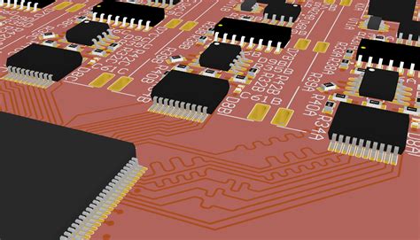
In the rapidly evolving world of advanced electronics, the demand for high-performance printed circuit boards (PCBs) has never been greater. As the backbone of electronic devices, PCBs play a crucial role in ensuring the reliability and efficiency of complex systems.
With technological advancements pushing the boundaries of what is possible, selecting the right PCB is paramount for engineers and designers aiming to achieve optimal performance. This article explores the top five high-performance PCBs that are setting new standards in the industry, offering insights into their unique features and applications.
To begin with, Rogers RO4000 series PCBs are renowned for their exceptional thermal management and electrical performance.
These laminates are engineered to meet the demands of high-frequency applications, making them ideal for RF and microwave circuits. The low dielectric loss and stable dielectric constant across a wide frequency range ensure minimal signal distortion, which is critical for maintaining signal integrity in high-speed communication systems. Furthermore, the RO4000 series offers excellent dimensional stability, which is essential for precision in multilayer board designs.
Transitioning to another top contender, the Isola FR408HR PCB material is highly regarded for its high glass transition temperature (Tg) and low coefficient of thermal expansion (CTE).
These properties make it particularly suitable for high-reliability applications where thermal cycling and mechanical stress are concerns. The FR408HR is often employed in aerospace and defense industries, where performance under extreme conditions is non-negotiable. Its ability to withstand high temperatures without compromising structural integrity ensures that it remains a preferred choice for mission-critical applications.
Next, the Taconic TLY series PCBs are celebrated for their low-loss characteristics and high thermal conductivity.
These features make them an excellent choice for applications requiring efficient heat dissipation, such as power amplifiers and LED lighting systems. The TLY series is also known for its ease of fabrication, which simplifies the manufacturing process and reduces production costs. This combination of performance and practicality makes Taconic TLY PCBs a popular option for designers seeking to balance efficiency with cost-effectiveness.
In addition, the Panasonic Megtron 6 series stands out for its superior high-speed and high-frequency performance.
With a low dielectric constant and low dissipation factor, Megtron 6 PCBs are designed to support the increasing data rates demanded by modern communication networks. Their ability to maintain signal integrity at high frequencies makes them indispensable in data centers and telecommunication infrastructure. Moreover, the Megtron 6 series offers excellent thermal reliability, ensuring consistent performance even in demanding environments.
Finally, the Nelco N7000-2 HT series is a high-performance PCB material that excels in high-temperature applications.
Its high Tg and low CTE make it suitable for use in automotive and industrial electronics, where exposure to harsh conditions is common. The N7000-2 HT series also provides excellent chemical resistance, which enhances its durability and longevity in challenging environments. This robustness, combined with its electrical performance, makes it a versatile choice for a wide range of advanced electronic applications.
In conclusion, the selection of a high-performance PCB is a critical decision that can significantly impact the success of an electronic device. Each of the PCBs discussed offers unique advantages tailored to specific applications, from high-frequency communication systems to high-reliability aerospace components. By understanding the distinct features and benefits of these top-performing PCBs, engineers and designers can make informed choices that align with their project requirements, ultimately driving innovation and excellence in the field of advanced electronics.
Comparing the Best PCBs for Consumer Electronics
In the rapidly evolving world of consumer electronics, the printed circuit board (PCB) stands as a fundamental component, serving as the backbone for most electronic devices. As technology advances, the demand for high-quality PCBs has surged, prompting manufacturers to innovate and improve their offerings. When comparing the best PCBs for consumer electronics, several factors come into play, including material quality, design complexity, and manufacturing precision. Understanding these elements is crucial for selecting the most suitable PCB for a given application.
To begin with, the material used in PCB fabrication significantly influences its performance and durability.
The most common substrate material is FR-4, a composite of woven fiberglass cloth with an epoxy resin binder that is flame resistant. FR-4 is favored for its excellent mechanical strength and electrical insulation properties, making it ideal for a wide range of consumer electronics. However, for applications requiring higher thermal performance, such as in high-power devices, manufacturers might opt for materials like polyimide or metal-core PCBs. These materials offer superior heat dissipation, ensuring the device operates efficiently under demanding conditions.
In addition to material considerations, the complexity of the PCB design is another critical factor.
As consumer electronics become more sophisticated, the need for multi-layer PCBs has increased. Multi-layer PCBs allow for more intricate circuit designs, accommodating the growing number of components in modern devices. This complexity enables manufacturers to produce smaller, more compact devices without compromising functionality. However, designing multi-layer PCBs requires advanced software tools and expertise, as well as precise manufacturing processes to ensure reliability and performance.
Moreover, the precision of the manufacturing process is paramount in determining the quality of a PCB.
Advanced fabrication techniques, such as surface mount technology (SMT) and through-hole technology, play a vital role in the assembly of PCBs. SMT, in particular, has become the preferred method for assembling components on PCBs due to its ability to place components on both sides of the board, thus maximizing space efficiency. This method also supports the miniaturization trend in consumer electronics, allowing for the production of smaller and lighter devices.
Furthermore, the choice of PCB manufacturer can greatly impact the final product’s quality.
Leading manufacturers invest in state-of-the-art equipment and adhere to stringent quality control standards to ensure their PCBs meet industry specifications. They also offer a range of services, from prototyping to mass production, providing flexibility to accommodate different project needs. Collaborating with a reputable manufacturer can result in a PCB that not only meets but exceeds performance expectations.
In conclusion, selecting the best PCB for consumer electronics involves a careful evaluation of material quality, design complexity, and manufacturing precision. As technology continues to advance, the demand for high-performance PCBs will only grow, driving further innovation in the industry. By understanding the key factors that contribute to a PCB’s quality, manufacturers and designers can make informed decisions that enhance the functionality and reliability of their electronic devices. As a result, consumers can enjoy more efficient, durable, and sophisticated electronics that meet the demands of modern life.
Innovative PCB Designs for IoT Applications
In the rapidly evolving landscape of the Internet of Things (IoT), the demand for innovative printed circuit board (PCB) designs has surged, driven by the need for compact, efficient, and reliable solutions. As IoT devices become increasingly ubiquitous, the role of PCBs in ensuring seamless connectivity and functionality cannot be overstated. These boards serve as the backbone of IoT devices, facilitating the integration of various components and enabling the transmission of data across networks. Consequently, the development of advanced PCB designs tailored for IoT applications has become a focal point for engineers and manufacturers alike.
One of the most significant trends in PCB design for IoT applications is miniaturization.
As IoT devices are often required to be small and portable, the PCBs within them must also be compact. This has led to the adoption of high-density interconnect (HDI) technology, which allows for more components to be placed on a smaller board without compromising performance. HDI PCBs utilize microvias, blind vias, and buried vias to create more routing space, thereby enabling the integration of complex circuits in a limited area. This innovation not only supports the miniaturization of devices but also enhances their functionality by accommodating more features.
In addition to miniaturization, flexibility is another crucial aspect of PCB design for IoT applications.
Flexible PCBs, or flex PCBs, are increasingly being used in IoT devices due to their ability to bend and conform to various shapes. This flexibility is particularly advantageous in wearable technology, where the PCB must adapt to the contours of the human body. Flex PCBs are made from materials such as polyimide, which provide durability and resilience while maintaining a lightweight profile. The use of flex PCBs in IoT devices not only improves their ergonomic design but also enhances their durability by reducing the risk of damage from mechanical stress.
Moreover, the integration of advanced materials and technologies in PCB design is paving the way for more efficient IoT devices.
For instance, the use of low-loss materials in PCBs helps reduce signal attenuation, thereby improving the performance of high-frequency applications. Additionally, the incorporation of embedded components, such as resistors and capacitors, directly into the PCB substrate can further optimize space and enhance electrical performance. These innovations contribute to the development of PCBs that are not only smaller and more flexible but also more efficient and reliable.
Furthermore, the rise of smart manufacturing techniques, such as additive manufacturing and 3D printing, is revolutionizing PCB production for IoT applications.
These techniques allow for rapid prototyping and customization, enabling manufacturers to quickly adapt to the specific requirements of different IoT devices. By leveraging these advanced manufacturing processes, companies can produce PCBs with intricate designs and complex geometries that were previously unattainable with traditional methods. This capability is particularly beneficial in the IoT sector, where the diversity of applications demands a wide range of PCB configurations.
In conclusion, the development of innovative PCB designs is crucial for the advancement of IoT technology. Through miniaturization, flexibility, the integration of advanced materials, and the adoption of smart manufacturing techniques, PCBs are becoming more capable of meeting the demands of modern IoT applications. As the IoT ecosystem continues to expand, the role of PCBs in enabling connectivity and functionality will remain indispensable, driving further innovation in this critical area of technology.
The Future of PCBs: Trends and Technologies to Watch
The future of printed circuit boards (PCBs) is poised for significant transformation as emerging trends and technologies continue to reshape the landscape of electronics manufacturing. As the backbone of modern electronic devices, PCBs are integral to the functionality and performance of a wide array of products, from consumer electronics to industrial machinery. Consequently, advancements in PCB technology are crucial for driving innovation across various sectors.
One of the most notable trends in the PCB industry is the increasing demand for miniaturization.
As electronic devices become more compact and portable, there is a growing need for smaller, more efficient PCBs. This trend is particularly evident in the consumer electronics market, where smartphones, wearables, and other portable devices require highly compact and densely packed circuit boards. To meet this demand, manufacturers are exploring advanced materials and fabrication techniques that allow for the production of thinner and lighter PCBs without compromising performance.
In addition to miniaturization, the push for greater functionality is driving the development of multi-layer PCBs.
These boards, which consist of multiple layers of circuitry stacked on top of one another, enable more complex and powerful electronic devices. By increasing the number of layers, manufacturers can incorporate more components and connections into a single board, thereby enhancing the device’s capabilities.
This trend is particularly relevant in industries such as telecommunications and computing, where the need for high-performance devices is paramount.
Furthermore, the rise of the Internet of Things (IoT) is significantly influencing PCB design and manufacturing. As more devices become interconnected, there is a growing need for PCBs that can support wireless communication and data transfer. This has led to the development of PCBs with integrated antennas and other wireless components, enabling seamless connectivity between devices. The IoT trend is expected to continue driving innovation in PCB technology, as manufacturers strive to create boards that can support the ever-expanding network of connected devices.
Another key trend shaping the future of PCBs is the increasing emphasis on sustainability and environmental responsibility.
As concerns about electronic waste and resource consumption grow, manufacturers are seeking ways to reduce the environmental impact of PCB production. This includes the use of eco-friendly materials, such as biodegradable substrates and lead-free solder, as well as the implementation of energy-efficient manufacturing processes. By prioritizing sustainability, the PCB industry can contribute to a more sustainable future while meeting the demands of environmentally conscious consumers. Moreover, advancements in materials science are opening new possibilities for PCB design and functionality. The development of flexible and stretchable PCBs, for example, is enabling the creation of innovative electronic devices that can conform to various shapes and surfaces. These flexible boards are particularly useful in applications such as wearable technology and medical devices, where traditional rigid PCBs may not be suitable. As research in this area continues to progress, it is likely that flexible PCBs will become increasingly prevalent in a wide range of applications.
In conclusion, the future of PCBs is being shaped by a variety of trends and technologies that are driving innovation and transforming the electronics industry. From miniaturization and multi-layer designs to IoT integration and sustainability, these developments are paving the way for more advanced and efficient electronic devices. As the demand for cutting-edge technology continues to grow, the PCB industry will undoubtedly play a crucial role in meeting the needs of consumers and businesses alike. By staying at the forefront of these trends, manufacturers can ensure that they remain competitive in an ever-evolving market.


