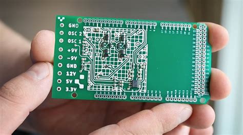
Beta layout flex pcb
Advantages Of Using Flex PCBs In Beta Layout Designs
In the realm of modern electronics, the demand for more compact, efficient, and versatile devices has led to significant advancements in printed circuit board (PCB) technology. Among these innovations, flexible PCBs, or flex PCBs, have emerged as a pivotal component in beta layout designs. These flexible circuits offer a multitude of advantages that make them an attractive choice for engineers and designers aiming to optimize their electronic products.
To begin with, one of the most notable advantages of using flex PCBs in beta layout designs is their inherent flexibility.
Unlike traditional rigid PCBs, flex PCBs can be bent, folded, and twisted without compromising their functionality. This flexibility allows for more creative and efficient use of space within electronic devices, enabling designers to develop more compact and lightweight products. As a result, flex PCBs are particularly beneficial in applications where space is at a premium, such as in wearable technology, medical devices, and compact consumer electronics.
Moreover, the use of flex PCBs in beta layout designs enhances the reliability and durability of electronic products.
The flexible nature of these circuits allows them to absorb and withstand mechanical stress and vibrations more effectively than their rigid counterparts. This characteristic is especially advantageous in environments where electronic devices are subject to constant movement or harsh conditions, such as in automotive and aerospace applications. By reducing the risk of circuit failure due to mechanical stress, flex PCBs contribute to the overall longevity and performance of the device.
In addition to their mechanical benefits, flex PCBs also offer significant electrical advantages.
The ability to design circuits with three-dimensional configurations allows for shorter and more direct electrical paths. This can lead to improved signal integrity and reduced electromagnetic interference, which are critical factors in high-frequency applications. Furthermore, the reduced need for connectors and interconnects in flex PCB designs minimizes potential points of failure and enhances the overall electrical performance of the device.
Another compelling advantage of flex PCBs in beta layout designs is their potential for cost savings.
While the initial design and manufacturing costs of flex PCBs may be higher than those of traditional rigid PCBs, the long-term benefits often outweigh these initial expenses. The reduction in the number of components, connectors, and interconnects not only simplifies assembly processes but also decreases the likelihood of assembly errors. This simplification can lead to lower production costs and faster time-to-market for new products, providing a competitive edge in the fast-paced electronics industry.
Furthermore, the versatility of flex PCBs allows for greater design freedom and innovation.
Designers can explore unconventional shapes and configurations that would be impossible with rigid PCBs, opening up new possibilities for product development. This adaptability is particularly valuable in beta layout designs, where rapid prototyping and iterative testing are essential. Flex PCBs enable designers to quickly implement changes and improvements, facilitating a more efficient and effective design process.
In conclusion, the advantages of using flex PCBs in beta layout designs are manifold. Their flexibility, reliability, electrical performance, cost-effectiveness, and design versatility make them an indispensable tool for modern electronic design. As technology continues to evolve, the role of flex PCBs in enabling innovative and efficient electronic products is likely to become even more pronounced, solidifying their place as a cornerstone of advanced PCB technology.
Key Considerations For Designing Flex PCBs In Beta Layout
Designing flexible printed circuit boards (flex PCBs) in a beta layout stage involves a meticulous process that requires careful consideration of various factors to ensure optimal performance and reliability. As the demand for compact and versatile electronic devices continues to grow, flex PCBs have become increasingly popular due to their ability to bend and conform to different shapes, making them ideal for applications where space is limited. However, the unique properties of flex PCBs necessitate a distinct approach to design, particularly during the beta layout phase, where the focus is on refining and optimizing the initial design.
One of the primary considerations in designing flex PCBs is the choice of materials.
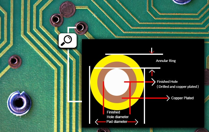
Unlike rigid PCBs, flex PCBs are made from flexible substrates such as polyimide, which provide the necessary flexibility and durability. The selection of the appropriate substrate material is crucial, as it directly impacts the board’s ability to withstand mechanical stress and environmental factors. Additionally, the thickness of the substrate must be carefully chosen to balance flexibility with the required electrical performance. As such, designers must evaluate the specific requirements of the application to determine the most suitable material and thickness.
Another critical aspect is the layout of the circuit traces.
In flex PCBs, the traces must be designed to accommodate bending and flexing without compromising electrical integrity. This involves using curved traces instead of sharp angles, which can create stress points and lead to potential failure. Furthermore, the width and spacing of the traces should be optimized to prevent issues such as impedance mismatches and signal loss. During the beta layout stage, designers often employ simulation tools to model the behavior of the circuit under various conditions, allowing them to make informed adjustments to the trace layout.
The placement of components is also a key consideration in flex PCB design.
Due to the flexible nature of the board, components must be strategically positioned to minimize stress during bending. This often involves placing components in areas that experience the least amount of flexing or using reinforcement techniques such as stiffeners to provide additional support. Moreover, the orientation of components should be carefully planned to ensure that they do not interfere with the board’s ability to flex. In the beta layout phase, designers may create prototypes to test different component placements and assess their impact on the board’s performance.
Thermal management is another important factor to consider when designing flex PCBs.
The flexible substrate materials used in these boards typically have lower thermal conductivity compared to rigid boards, which can lead to heat buildup and potential damage to components. To address this, designers must incorporate effective thermal management strategies, such as using thermal vias or heat sinks, to dissipate heat efficiently. During the beta layout stage, thermal analysis tools can be employed to identify potential hotspots and optimize the design accordingly.
In conclusion, designing flex PCBs in a beta layout requires a comprehensive understanding of the unique challenges and considerations associated with flexible circuits. By carefully selecting materials, optimizing trace layouts, strategically placing components, and implementing effective thermal management strategies, designers can create flex PCBs that meet the demanding requirements of modern electronic applications. As technology continues to evolve, the ability to design reliable and efficient flex PCBs will remain a critical skill for engineers and designers in the electronics industry.
Innovations In Beta Layout Flex PCB Technology
Beta layout flex PCB technology has emerged as a pivotal innovation in the electronics industry, offering a versatile solution to the ever-evolving demands of modern electronic devices. As the demand for smaller, more efficient, and highly reliable electronic components continues to grow, the development of flexible printed circuit boards (PCBs) has become increasingly significant. These flexible PCBs, often referred to as flex PCBs, are designed to meet the challenges posed by the need for compact and lightweight electronic devices, while also providing enhanced performance and durability.
One of the primary advantages of beta layout flex PCB technology is its ability to conform to complex shapes and fit into tight spaces, which is particularly beneficial in applications where traditional rigid PCBs would be impractical.
This flexibility is achieved through the use of thin, flexible substrates that can bend and twist without compromising the integrity of the electrical connections. Consequently, flex PCBs are ideal for use in a wide range of applications, from consumer electronics such as smartphones and wearable devices to more demanding environments like automotive and aerospace industries.
Moreover, the innovation in beta layout flex PCB technology has led to significant improvements in the reliability and performance of electronic devices. By allowing for more efficient use of space and reducing the need for connectors and cables, flex PCBs minimize the risk of mechanical failure and improve signal integrity. This is particularly important in high-frequency applications, where maintaining signal quality is crucial. Additionally, the reduced weight and size of flex PCBs contribute to the overall efficiency and portability of electronic devices, making them an attractive option for manufacturers seeking to optimize their products.
In addition to their physical advantages, beta layout flex PCBs also offer significant benefits in terms of manufacturing and assembly.
The ability to produce complex circuits on a single flexible substrate simplifies the assembly process and reduces the number of components required, leading to cost savings and increased production efficiency. Furthermore, advancements in materials and fabrication techniques have enhanced the durability and thermal performance of flex PCBs, making them suitable for use in harsh environments where traditional PCBs might fail.
As the technology continues to evolve, the integration of beta layout flex PCBs with other emerging technologies is opening up new possibilities for innovation. For instance, the combination of flex PCBs with advanced sensor technologies is enabling the development of smart textiles and wearable health monitoring devices, which require flexible and lightweight electronic components. Similarly, the integration of flex PCBs with Internet of Things (IoT) devices is facilitating the creation of more compact and efficient systems, capable of operating in a variety of environments.
In conclusion, the advancements in beta layout flex PCB technology are playing a crucial role in shaping the future of electronics.
By offering a flexible, reliable, and efficient solution to the challenges posed by modern electronic devices, flex PCBs are enabling the development of innovative products that meet the demands of today’s consumers. As research and development in this field continue to progress, it is likely that we will see even more exciting applications and improvements in the capabilities of flex PCBs, further solidifying their position as a key component in the electronics industry.
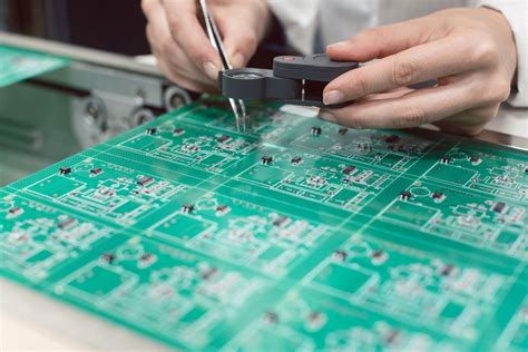
Common Challenges And Solutions In Beta Layout Flex PCB Manufacturing
In the realm of modern electronics, the demand for compact, lightweight, and flexible devices has led to the increased adoption of flexible printed circuit boards (PCBs). Among the various stages of PCB development, the beta layout phase is crucial, as it serves as a bridge between the initial design and full-scale production. However, this phase is not without its challenges. Understanding these common challenges and their solutions is essential for manufacturers aiming to optimize the beta layout flex PCB manufacturing process.
One of the primary challenges in beta layout flex PCB manufacturing is ensuring the reliability and durability of the flexible circuits.
Flex PCBs are often subjected to mechanical stress due to their bending and folding capabilities. This can lead to issues such as delamination, cracking, or tearing of the conductive traces. To address this, manufacturers can employ advanced materials and design techniques. For instance, using polyimide substrates, known for their excellent thermal stability and mechanical strength, can significantly enhance the durability of flex PCBs. Additionally, incorporating strain relief features in the design can help distribute mechanical stress more evenly, reducing the risk of damage.
Another significant challenge is maintaining signal integrity in the flexible circuits.
As devices become more complex, the need for high-speed data transmission increases, making signal integrity a critical concern. Flex PCBs, with their unique geometries and material properties, can introduce issues such as impedance mismatches and electromagnetic interference. To mitigate these problems, manufacturers can utilize controlled impedance design techniques and incorporate shielding layers within the PCB stack-up. Moreover, employing simulation tools during the beta layout phase can help identify potential signal integrity issues early in the design process, allowing for timely adjustments.
Thermal management is also a crucial consideration in the beta layout flex PCB manufacturing process.
Flexible circuits are often used in compact devices where heat dissipation is a challenge. Excessive heat can lead to performance degradation or even failure of the electronic components. To combat this, manufacturers can integrate thermal vias and heat spreaders into the PCB design to facilitate efficient heat dissipation. Additionally, selecting materials with high thermal conductivity can further enhance the thermal performance of flex PCBs.
Manufacturability is another aspect that poses challenges during the beta layout phase.
The intricate designs and fine features of flex PCBs can complicate the manufacturing process, leading to increased production costs and time. To overcome these challenges, manufacturers can adopt design for manufacturability (DFM) principles. This involves optimizing the PCB layout to simplify the manufacturing process, such as minimizing the number of layers and ensuring adequate spacing between traces. Collaborating closely with PCB fabricators during the beta layout phase can also provide valuable insights into potential manufacturing constraints and help refine the design accordingly.
In conclusion, while the beta layout flex PCB manufacturing process presents several challenges, understanding and addressing these issues is key to achieving a successful outcome.
By focusing on enhancing reliability, maintaining signal integrity, managing thermal performance, and optimizing manufacturability, manufacturers can effectively navigate the complexities of flex PCB production. As technology continues to evolve, staying abreast of the latest advancements and best practices in flex PCB design and manufacturing will be essential for meeting the demands of the ever-changing electronics landscape.