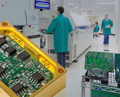
Bga on flex pcb
Advantages Of Using BGA On Flex PCB In Modern Electronics
Ball Grid Array (BGA) technology, when integrated with flexible printed circuit boards (flex PCBs), offers a multitude of advantages that are increasingly being leveraged in modern electronics. As the demand for more compact, efficient, and reliable electronic devices continues to grow, the combination of BGA and flex PCBs emerges as a pivotal solution. This synergy not only addresses the challenges of miniaturization but also enhances the performance and durability of electronic components.
To begin with, one of the primary advantages of using BGA on flex PCBs is the significant reduction in size and weight.
BGA packages are known for their ability to accommodate a high number of interconnections in a relatively small footprint. This is particularly beneficial in applications where space is at a premium, such as in smartphones, wearable devices, and other portable electronics. The use of flex PCBs further complements this advantage by allowing the circuit to conform to complex shapes and fit into tight spaces, thus enabling more innovative and ergonomic product designs.
Moreover, the combination of BGA and flex PCBs enhances thermal management, which is a critical consideration in modern electronics.
BGA packages facilitate efficient heat dissipation due to their design, which allows for a larger surface area in contact with the PCB. When paired with the inherent flexibility and thermal properties of flex PCBs, this results in improved heat distribution and reduced risk of overheating. Consequently, devices can operate at higher speeds and with greater reliability, which is essential for maintaining performance in demanding applications.
In addition to thermal management, the electrical performance of devices is also improved through the use of BGA on flex PCBs.
The short and direct interconnections provided by BGA packages minimize signal distortion and electromagnetic interference, leading to faster signal transmission and enhanced overall performance. Flex PCBs contribute to this by offering low inductance and capacitance, which are crucial for maintaining signal integrity in high-frequency applications. This makes the combination particularly advantageous in sectors such as telecommunications and computing, where high-speed data processing is paramount.
Furthermore, the durability and reliability of electronic devices are significantly bolstered by employing BGA on flex PCBs.
The robust nature of BGA connections, which are less prone to mechanical stress compared to traditional leaded packages, ensures a longer lifespan for the components. Flex PCBs add to this resilience by providing excellent resistance to vibration and mechanical fatigue, making them ideal for use in environments subject to constant movement or harsh conditions. This reliability is especially important in automotive and aerospace industries, where failure is not an option.
Finally, the manufacturing process benefits from the integration of BGA on flex PCBs.
The automated assembly of BGA components is streamlined and cost-effective, reducing production time and minimizing errors. Flex PCBs, with their ability to reduce the number of connectors and interconnects required, further simplify the assembly process and lower production costs. This efficiency in manufacturing translates to more affordable and accessible electronic products for consumers.
In conclusion, the advantages of using BGA on flex PCBs in modern electronics are manifold, encompassing size reduction, enhanced thermal and electrical performance, increased durability, and manufacturing efficiency. As technology continues to evolve, the integration of these two innovations will undoubtedly play a crucial role in shaping the future of electronic device design and functionality.
Design Considerations For Implementing BGA On Flex PCB
When designing with Ball Grid Arrays (BGAs) on flexible printed circuit boards (flex PCBs), several critical considerations must be addressed to ensure optimal performance and reliability. The integration of BGAs on flex PCBs presents unique challenges due to the inherent properties of flexible substrates, which differ significantly from rigid boards. Therefore, understanding these nuances is essential for engineers and designers aiming to leverage the advantages of flex PCBs while maintaining the integrity of BGA components.
To begin with, the choice of materials plays a pivotal role in the successful implementation of BGAs on flex PCBs.
Flex PCBs are typically made from polyimide, a material known for its flexibility and thermal stability. However, the thermal expansion properties of polyimide differ from those of the BGA solder balls, which can lead to mechanical stress during thermal cycling. To mitigate this, it is crucial to select materials with compatible coefficients of thermal expansion (CTE) to minimize stress and potential solder joint failure.
Moreover, the layout and design of the flex PCB must be meticulously planned.
The routing of traces and the placement of vias should be optimized to reduce stress concentrations and enhance mechanical stability. It is advisable to avoid sharp bends and to maintain a uniform trace width to prevent stress fractures. Additionally, the use of teardrop pads can help distribute stress more evenly around vias and solder joints, thereby improving the overall durability of the assembly.
Thermal management is another critical aspect to consider when implementing BGAs on flex PCBs.
The flexible nature of these boards can lead to challenges in heat dissipation, which is particularly important for high-density BGA packages. Incorporating thermal vias and heat spreaders can aid in managing heat effectively. Furthermore, designers should consider the use of thermal reliefs in the pad design to balance the heat distribution during soldering, which can prevent warping and ensure a reliable solder joint.
The soldering process itself requires careful attention.
Flex PCBs are more susceptible to warping during reflow soldering due to their thin and flexible nature. To address this, it is essential to use a reflow profile that minimizes thermal shock and ensures even heating across the board. Additionally, the use of low-temperature solder paste can reduce the risk of damage to the flex PCB and the BGA components.
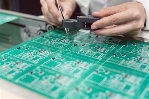
Testing and inspection are indispensable in the design process to ensure the reliability of BGAs on flex PCBs.
Non-destructive testing methods, such as X-ray inspection, can be employed to verify the integrity of solder joints and detect any potential defects. Furthermore, implementing design for testability (DFT) principles can facilitate easier testing and troubleshooting, thereby enhancing the overall reliability of the final product.
In conclusion, the successful implementation of BGAs on flex PCBs requires a comprehensive understanding of the interplay between materials, design, thermal management, and soldering processes. By carefully considering these factors, designers can overcome the challenges associated with flex PCBs and harness their benefits, such as reduced weight and increased flexibility, without compromising the performance and reliability of BGA components. As technology continues to advance, the demand for innovative solutions in this area will undoubtedly grow, making it imperative for designers to stay informed and adapt to emerging trends and techniques.
Challenges And Solutions In BGA Assembly On Flex PCB
Ball Grid Array (BGA) assembly on flexible printed circuit boards (flex PCBs) presents a unique set of challenges and solutions that are critical to the advancement of modern electronics. As the demand for smaller, lighter, and more versatile electronic devices continues to grow, the integration of BGA components on flex PCBs has become increasingly prevalent. However, this integration is not without its difficulties, primarily due to the inherent characteristics of both BGA packages and flex PCBs.
One of the primary challenges in BGA assembly on flex PCBs is the alignment and placement accuracy.
BGA packages, known for their high-density interconnections, require precise alignment to ensure reliable electrical connections. The flexible nature of the substrate can complicate this process, as it is more prone to warping and movement during assembly compared to rigid PCBs. To address this issue, advanced placement equipment with high precision and vision systems is often employed. These systems can accurately position the BGA components, compensating for any substrate movement and ensuring proper alignment.
In addition to alignment challenges, the thermal management during the soldering process is another significant concern.
Flex PCBs have different thermal properties compared to their rigid counterparts, which can affect the reflow soldering process used to attach BGA components. The flexible substrate may not dissipate heat as effectively, leading to uneven temperature distribution and potential soldering defects such as voids or incomplete solder joints. To mitigate these risks, careful thermal profiling is essential. This involves optimizing the reflow oven settings to ensure uniform heat distribution across the flex PCB, thereby achieving consistent soldering results.
Moreover, the mechanical properties of flex PCBs introduce additional challenges in terms of reliability and durability.
The flexibility that makes these PCBs desirable for certain applications also makes them susceptible to mechanical stress and fatigue. BGA components, with their numerous solder balls, can be particularly vulnerable to these stresses, which may lead to joint failure over time. To enhance the mechanical reliability of BGA assemblies on flex PCBs, designers often incorporate strain relief features and select materials with appropriate flexibility and strength. Additionally, rigorous testing and validation processes are implemented to ensure that the assemblies can withstand the mechanical demands of their intended applications.
Furthermore, the inspection and testing of BGA assemblies on flex PCBs pose their own set of challenges.
Traditional inspection methods, such as visual inspection and X-ray analysis, may be less effective due to the flexible nature of the substrate and the dense arrangement of solder balls. Advanced inspection techniques, including automated optical inspection (AOI) and 3D X-ray imaging, are increasingly utilized to overcome these limitations. These technologies provide detailed insights into the quality of solder joints and the overall integrity of the assembly, enabling manufacturers to identify and address potential issues before they lead to failures in the field.
In conclusion, while BGA assembly on flex PCBs presents several challenges, advancements in technology and process optimization have provided effective solutions. By addressing alignment, thermal management, mechanical reliability, and inspection challenges, manufacturers can successfully integrate BGA components onto flex PCBs, paving the way for innovative electronic devices that meet the demands of modern consumers. As the industry continues to evolve, ongoing research and development will undoubtedly yield further improvements, ensuring that the integration of BGA on flex PCBs remains a viable and reliable option for future applications.
Future Trends In BGA Technology For Flexible PCBs
Ball Grid Array (BGA) technology has long been a cornerstone in the realm of electronic packaging, offering a compact and efficient solution for mounting integrated circuits. As the demand for more sophisticated and miniaturized electronic devices continues to grow, the integration of BGA technology with flexible printed circuit boards (PCBs) is becoming increasingly significant. This convergence is not only enhancing the performance and reliability of electronic devices but also paving the way for innovative applications across various industries. In this context, exploring the future trends in BGA technology for flexible PCBs reveals a landscape rich with potential advancements and challenges.
To begin with, the miniaturization of electronic components is a trend that shows no signs of abating.
As devices become smaller, the need for compact and efficient packaging solutions becomes paramount. BGA technology, with its ability to provide high-density interconnections, is ideally suited to meet this demand. When combined with flexible PCBs, which offer the advantage of bending and folding to fit into tight spaces, the potential for creating ultra-compact devices is significantly enhanced. This synergy is particularly beneficial in the development of wearable technology, where space is at a premium and flexibility is essential.
Moreover, the rise of the Internet of Things (IoT) is driving the need for more robust and versatile electronic components.
Flexible PCBs equipped with BGA technology are well-positioned to support this trend, as they can be integrated into a wide array of IoT devices, from smart home appliances to industrial sensors. The ability of flexible PCBs to withstand mechanical stress and environmental factors makes them ideal for IoT applications, where reliability and durability are critical. As IoT continues to expand, the demand for flexible PCBs with advanced BGA technology is expected to grow exponentially.
In addition to miniaturization and IoT, the push for higher performance and efficiency is another key trend shaping the future of BGA technology on flexible PCBs.
As electronic devices become more complex, the need for faster data transmission and improved thermal management becomes increasingly important. BGA packages, with their short electrical paths and excellent heat dissipation properties, are well-suited to address these challenges. Furthermore, advancements in materials and manufacturing processes are enabling the development of BGAs with even greater performance capabilities. For instance, the use of advanced substrates and innovative soldering techniques is enhancing the electrical and thermal performance of BGA packages on flexible PCBs.
However, the integration of BGA technology with flexible PCBs is not without its challenges.
The complexity of manufacturing and assembling these components requires precise control and expertise. Ensuring the reliability of solder joints, particularly in flexible applications, is a critical concern that must be addressed to prevent failures. Additionally, as devices become more compact, the risk of signal interference and crosstalk increases, necessitating careful design and layout considerations.
In conclusion, the future of BGA technology for flexible PCBs is poised for significant growth, driven by trends such as miniaturization, the proliferation of IoT, and the demand for higher performance. While challenges remain, ongoing advancements in materials, design, and manufacturing processes are paving the way for innovative solutions that will continue to push the boundaries of what is possible in electronic packaging. As these technologies evolve, they will undoubtedly play a crucial role in shaping the next generation of electronic devices, offering new possibilities for innovation and application across a wide range of industries.