Blind Vias in PCB Design: A Comprehensive Guide
1. Introduction to Blind Vias in PCBs
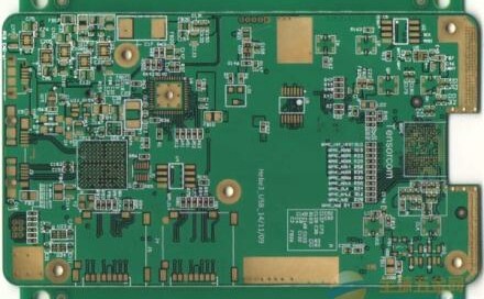
Printed Circuit Boards (PCBs) are essential components in modern electronics, enabling the interconnection of various electronic components. As electronic devices become more compact and complex, PCB designs must accommodate higher component densities and faster signal transmission. One critical aspect of advanced PCB design is the use of blind vias, which play a significant role in high-density interconnect (HDI) PCBs.
A blind via is a type of via that connects an outer layer of the PCB to one or more inner layers but does not go through the entire board. Unlike through-hole vias, which span from the top to the bottom layer, blind vias are only partially drilled, making them ideal for multilayer PCBs where space optimization is crucial.
This article explores blind vias in detail, covering their structure, manufacturing processes, advantages, challenges, and applications in modern PCB design.
2. Structure and Types of Blind Vias
2.1 Definition and Characteristics
A blind via is a plated hole that starts on an outer layer (top or bottom) and terminates at an internal layer without penetrating the entire board. These vias allow connections between surface layers and inner layers without occupying unnecessary space.
2.2 Types of Blind Vias
Blind vias can be categorized based on their depth and structure:
- Standard Blind Via: Connects the outer layer to the immediate inner layer.
- Buried Blind Via: Connects two or more inner layers but does not reach the outer layers.
- Stacked Blind Via: Multiple blind vias stacked on top of each other to create deeper connections.
- Staggered Blind Via: Blind vias offset from each other to avoid overlapping.
2.3 Comparison with Other Via Types
- Through-hole vias: Span the entire PCB, suitable for simpler designs but consume more space.
- Microvias: Smaller than traditional vias, often used in HDI PCBs, and can be blind or buried.
- Buried vias: Exist only between inner layers and are not visible from the surface.
3. Manufacturing Processes for Blind Vias
Creating blind vias requires precision and specialized techniques. The most common manufacturing methods include:
3.1 Laser Drilling
- Uses a high-precision laser (CO₂ or UV) to ablate the dielectric material.
- Ideal for small-diameter blind vias (microvias).
- Provides high accuracy and is suitable for HDI PCBs.
3.2 Mechanical Drilling
- Traditional drilling method using a CNC drill bit.
- Suitable for larger blind vias but less precise than laser drilling.
- May require additional plating and filling processes.
3.3 Sequential Lamination
- Involves building the PCB layer-by-layer, drilling blind vias at each stage.
- Ensures proper alignment between layers.
- Used for complex multilayer PCBs.
3.4 Plating and Filling
- After drilling, the via is plated with copper to ensure conductivity.
- May be filled with conductive or non-conductive epoxy to improve reliability.
4. Advantages of Using Blind Vias
Blind vias offer several benefits in PCB design:
4.1 Space Efficiency
- Allow for higher component density by reducing via footprint.
- Enable more routing channels in multilayer PCBs.
4.2 Improved Signal Integrity
- Shorter electrical paths reduce signal loss and crosstalk.
- Beneficial for high-speed and RF applications.
4.3 Enhanced Thermal Management
- Reduce thermal resistance by providing direct heat dissipation paths.
4.4 Design Flexibility
- Enable complex routing in HDI PCBs.
- Support advanced packaging techniques like flip-chip and BGA (Ball Grid Array).
5. Challenges and Limitations
Despite their advantages, blind vias present some challenges:
5.1 Higher Manufacturing Cost
- Requires advanced drilling and lamination techniques.
- More process steps increase production time and cost.
5.2 Reliability Concerns
- Potential for plating voids or incomplete filling.
- Thermal stress may cause cracks in stacked vias.
5.3 Design Complexity
- Requires precise layer alignment.
- Simulation and testing are critical to avoid signal integrity issues.
6. Applications of Blind Vias in Modern Electronics
Blind vias are widely used in advanced PCB applications, including:
6.1 Consumer Electronics
- Smartphones, tablets, and wearables where space is limited.
6.2 High-Speed Digital Circuits
- Servers, networking equipment, and data centers.
6.3 Automotive Electronics
- Advanced driver-assistance systems (ADAS) and infotainment systems.
6.4 Aerospace and Defense
- Avionics, radar systems, and satellite communications.
6.5 Medical Devices
- Miniaturized implants and diagnostic equipment.
7. Future Trends in Blind Via Technology
As PCBs continue to evolve, blind via technology is advancing in several ways:
7.1 Smaller and More Dense Vias
- Adoption of microvias (≤ 100 µm diameter) for ultra-HDI PCBs.
7.2 Advanced Materials
- Use of low-loss dielectrics for high-frequency applications.
7.3 3D Printed Electronics
- Additive manufacturing techniques for flexible and embedded PCBs.
7.4 Improved Reliability Testing
- Non-destructive inspection methods like 3D X-ray tomography.
8. Conclusion
Blind vias are a crucial element in modern PCB design, enabling higher density, better performance, and more compact electronic devices. While they introduce manufacturing and design challenges, their benefits in space savings, signal integrity, and thermal management make them indispensable in advanced applications such as HDI PCBs, high-speed circuits, and miniaturized electronics.
As technology progresses, innovations in laser drilling, material science, and additive manufacturing will further enhance the capabilities of blind vias, ensuring their continued relevance in next-generation PCB designs.