Blister pcb assembly
Understanding The Basics Of Blister PCB Assembly
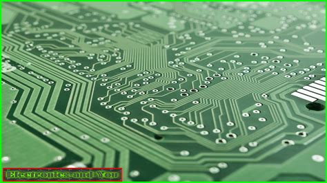
Blister PCB assembly is a critical process in the manufacturing of electronic devices, playing a pivotal role in ensuring the functionality and reliability of the final product. To understand the basics of blister PCB assembly, it is essential to first grasp the fundamental concept of what a printed circuit board (PCB) is.
A PCB serves as the backbone of most electronic devices, providing the necessary support and electrical connections for various components. The assembly process involves mounting electronic components onto the PCB, creating a functional electronic circuit.
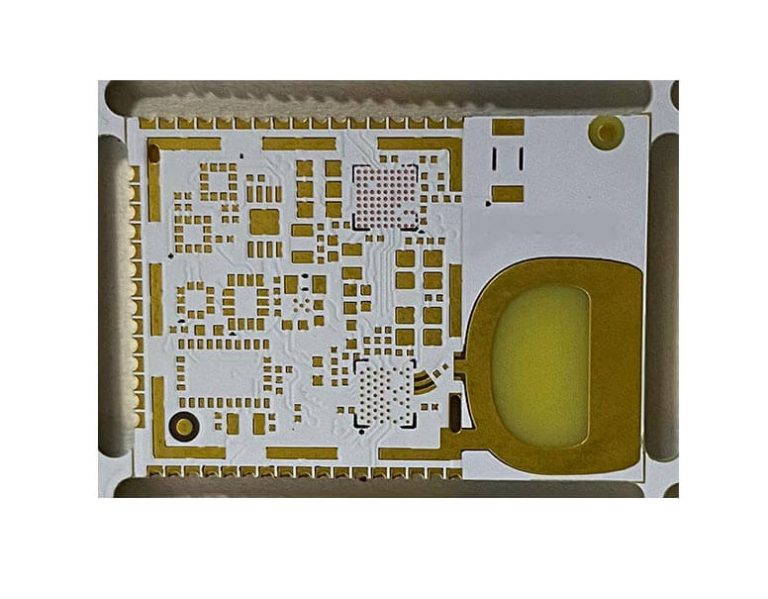
The term “blister” in blister PCB assembly refers to a specific defect that can occur during the manufacturing process.
This defect manifests as a raised area or bubble on the surface of the PCB, which can compromise the integrity and performance of the circuit. Blisters are typically caused by trapped air or moisture between the layers of the PCB during the lamination process. Understanding the causes and prevention of blisters is crucial for manufacturers aiming to produce high-quality PCBs.
To prevent blistering, manufacturers must ensure that the materials used in PCB production are of high quality and properly stored to avoid moisture absorption.
Additionally, the lamination process must be carefully controlled, with precise temperature and pressure settings to ensure that layers adhere correctly without trapping air or moisture. Regular inspection and testing during the manufacturing process can also help identify potential issues before they result in defects.
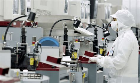
The assembly process itself involves several key steps, beginning with the application of solder paste to the PCB. This paste is applied to the areas where components will be mounted, serving as an adhesive that holds the components in place and provides the necessary electrical connections. Once the solder paste is applied, components are placed onto the PCB using automated machines that ensure precise positioning.
Following component placement, the PCB undergoes a reflow soldering process.
During this stage, the board is heated in a controlled environment, causing the solder paste to melt and form solid connections between the components and the PCB. This step is critical, as improper soldering can lead to weak connections and potential failures in the final product.
After soldering, the assembled PCB is subjected to a series of inspections and tests to ensure its functionality and reliability.
These tests may include visual inspections, automated optical inspections, and functional testing to verify that the circuit operates as intended. Any defects identified during these inspections must be addressed promptly to prevent faulty products from reaching the market.
In conclusion, understanding the basics of blister PCB assembly involves recognizing the importance of each step in the manufacturing process and the potential challenges that can arise. By focusing on quality control and adhering to best practices, manufacturers can minimize the risk of defects such as blisters and produce reliable, high-performance PCBs. As technology continues to advance, the demand for sophisticated electronic devices will only increase, making the mastery of PCB assembly techniques more crucial than ever. Through continuous improvement and innovation, the industry can meet these demands while maintaining the highest standards of quality and reliability.

Advantages Of Using Blister Packaging In PCB Assembly
Blister packaging has emerged as a pivotal component in the realm of printed circuit board (PCB) assembly, offering a multitude of advantages that enhance both the efficiency and reliability of the manufacturing process. As the demand for electronic devices continues to surge, manufacturers are increasingly turning to innovative packaging solutions to ensure the integrity and performance of their products. Blister packaging, in particular, stands out due to its unique ability to provide robust protection, streamline logistics, and facilitate quality control.
One of the primary advantages of using blister packaging in PCB assembly is its exceptional protective capabilities.
PCBs are inherently delicate and susceptible to damage from environmental factors such as moisture, dust, and static electricity. Blister packaging effectively shields these sensitive components from such hazards by encasing them in a secure, transparent plastic shell. This protective barrier not only prevents physical damage during transportation and handling but also mitigates the risk of contamination, thereby preserving the functionality and longevity of the PCBs.
In addition to its protective attributes, blister packaging significantly enhances the efficiency of the logistics process.
The uniformity and compactness of blister packs allow for optimal space utilization during storage and transportation. This streamlined packaging solution reduces the need for excessive cushioning materials, thereby minimizing waste and lowering shipping costs. Furthermore, the transparency of blister packaging enables easy identification and inspection of the contents without the need to open the package, facilitating faster inventory management and reducing the likelihood of errors.
Moreover, blister packaging plays a crucial role in quality control within PCB assembly.
The clear visibility of the packaged components allows for quick visual inspections, ensuring that any defects or discrepancies are promptly identified and addressed. This aspect is particularly beneficial in high-volume production environments where maintaining consistent quality is paramount. By enabling efficient quality checks, blister packaging helps manufacturers uphold stringent standards and deliver reliable products to their customers.
Transitioning to another significant advantage, blister packaging also contributes to enhanced branding and product presentation.
The customizable nature of blister packs allows manufacturers to incorporate branding elements such as logos, product information, and barcodes directly onto the packaging. This not only aids in brand recognition but also provides consumers with essential information about the product, thereby enhancing the overall customer experience. Additionally, the professional appearance of blister packaging can elevate the perceived value of the product, making it more appealing to consumers.
Furthermore, blister packaging is an environmentally conscious choice for PCB assembly.
Many blister packs are made from recyclable materials, aligning with the growing emphasis on sustainability within the electronics industry. By opting for eco-friendly packaging solutions, manufacturers can reduce their environmental footprint and appeal to environmentally conscious consumers. This commitment to sustainability not only benefits the planet but also enhances the brand’s reputation and marketability.
In conclusion, the advantages of using blister packaging in PCB assembly are manifold, encompassing protection, efficiency, quality control, branding, and sustainability. As the electronics industry continues to evolve, the adoption of innovative packaging solutions like blister packaging will undoubtedly play a crucial role in meeting the demands of modern manufacturing. By leveraging these benefits, manufacturers can ensure the delivery of high-quality, reliable products while simultaneously optimizing their operations and contributing to a more sustainable future.
Common Challenges In Blister PCB Assembly And How To Overcome Them
Blister PCB assembly, a critical process in the manufacturing of electronic devices, involves several intricate steps that can present numerous challenges. Understanding these challenges and implementing effective strategies to overcome them is essential for ensuring the reliability and performance of the final product.
One of the most common challenges in blister PCB assembly is the occurrence of soldering defects.
These defects, which include issues such as solder bridges, insufficient solder, and cold joints, can significantly impact the functionality of the PCB. To address these issues, it is crucial to maintain precise control over the soldering process. This can be achieved by optimizing the temperature profiles of reflow ovens and ensuring that solder paste is applied uniformly. Additionally, regular inspection and testing can help identify defects early in the process, allowing for timely corrective actions.
Another significant challenge in blister PCB assembly is the alignment of components.
Misalignment can lead to poor electrical connections and mechanical instability, which can compromise the performance of the device. To overcome this challenge, manufacturers can employ advanced pick-and-place machines equipped with vision systems. These systems can accurately position components on the PCB, reducing the likelihood of misalignment. Furthermore, implementing a robust quality control system that includes regular calibration of equipment can help maintain alignment accuracy over time.
The handling of delicate components during the assembly process also poses a challenge.
Components such as integrated circuits and capacitors are sensitive to electrostatic discharge (ESD) and physical damage. To mitigate these risks, it is essential to establish an ESD-safe environment by using antistatic materials and grounding systems. Additionally, training assembly line workers on proper handling techniques can further reduce the risk of damage to sensitive components.
Thermal management is another critical aspect of blister PCB assembly that can present challenges.
As electronic devices become more compact and powerful, managing the heat generated by components becomes increasingly important. Inadequate thermal management can lead to overheating, which can damage components and reduce the lifespan of the device. To address this issue, manufacturers can incorporate thermal vias, heat sinks, and thermal interface materials into the PCB design. These solutions help dissipate heat more effectively, ensuring that components operate within their specified temperature ranges.
Moreover, the complexity of modern PCBs, which often feature multiple layers and high-density interconnections, can complicate the assembly process.
This complexity can lead to difficulties in routing traces and ensuring signal integrity. To overcome these challenges, manufacturers can utilize advanced PCB design software that offers tools for optimizing trace routing and analyzing signal integrity. Collaborating closely with design engineers during the early stages of product development can also help identify potential issues and develop solutions before the assembly process begins.
Finally, supply chain disruptions can pose significant challenges in blister PCB assembly.
Delays in the availability of components can lead to production bottlenecks and increased costs. To mitigate these risks, manufacturers can establish strong relationships with multiple suppliers and maintain a buffer stock of critical components. Additionally, implementing a flexible production schedule can help accommodate changes in component availability, ensuring that assembly processes continue smoothly.
In conclusion, while blister PCB assembly presents several challenges, understanding these issues and implementing effective strategies can significantly enhance the quality and reliability of the final product. By focusing on soldering precision, component alignment, handling practices, thermal management, design complexity, and supply chain resilience, manufacturers can overcome these challenges and achieve successful PCB assembly.
Innovations In Blister PCB Assembly Technology
Blister PCB assembly technology has undergone significant advancements in recent years, driven by the increasing demand for more efficient, reliable, and compact electronic devices. As the electronics industry continues to evolve, the need for innovative solutions in printed circuit board (PCB) assembly becomes more critical. Blister PCB assembly, a method that involves the use of blister packaging techniques to protect and organize components, has emerged as a promising approach to address these challenges. This article explores the latest innovations in blister PCB assembly technology, highlighting how these developments are shaping the future of electronics manufacturing.
One of the most notable innovations in blister PCB assembly is the integration of automated processes.
Automation has revolutionized the manufacturing industry, and its impact on PCB assembly is no exception. By incorporating automated systems, manufacturers can achieve higher precision and consistency in the placement of components on PCBs. This not only reduces the likelihood of human error but also enhances the overall efficiency of the assembly process. Moreover, automated blister PCB assembly allows for faster production times, enabling manufacturers to meet the growing demand for electronic devices without compromising on quality.
In addition to automation, advancements in materials used for blister packaging have also contributed to the evolution of blister PCB assembly technology.
Traditionally, blister packaging was primarily made from plastic materials, which, while effective, posed environmental concerns due to their non-biodegradable nature. However, recent innovations have led to the development of eco-friendly materials that maintain the protective qualities of traditional blister packaging while minimizing environmental impact. These sustainable materials are not only beneficial for the environment but also align with the increasing consumer demand for greener products, thereby enhancing the marketability of devices utilizing blister PCB assembly.
Furthermore, the miniaturization of electronic components has necessitated the development of more sophisticated blister PCB assembly techniques.
As devices become smaller and more complex, the need for precise and reliable assembly methods becomes paramount. Innovations in micro-blister packaging have enabled manufacturers to accommodate the shrinking size of components without sacrificing performance or reliability. This advancement is particularly significant in industries such as consumer electronics and medical devices, where space constraints and functionality are critical considerations.
Another key innovation in blister PCB assembly technology is the incorporation of advanced inspection and testing methods.
Ensuring the quality and reliability of assembled PCBs is crucial, especially in applications where failure is not an option. Modern blister PCB assembly processes now include sophisticated inspection techniques, such as automated optical inspection (AOI) and X-ray inspection, to detect defects and ensure the integrity of the assembly. These technologies provide manufacturers with the ability to identify and rectify issues early in the production process, thereby reducing waste and improving overall product quality.
In conclusion, the innovations in blister PCB assembly technology are transforming the landscape of electronics manufacturing. Through the integration of automation, the use of sustainable materials, advancements in miniaturization techniques, and the implementation of advanced inspection methods, blister PCB assembly is becoming more efficient, reliable, and environmentally friendly. As the demand for compact and high-performance electronic devices continues to rise, these innovations will play a crucial role in meeting industry needs and driving future advancements. The ongoing evolution of blister PCB assembly technology promises to deliver even greater efficiencies and capabilities, paving the way for the next generation of electronic devices.