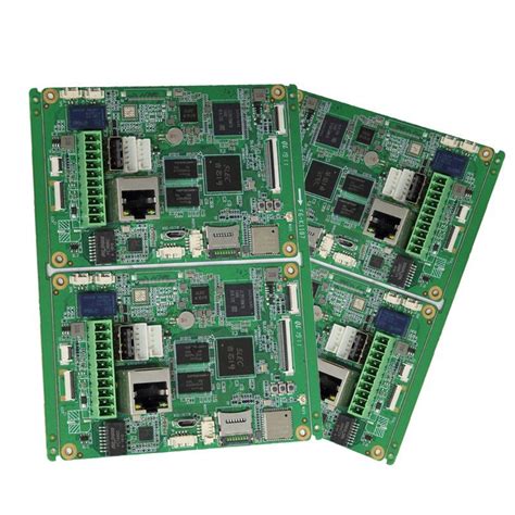
Board assembly
Innovations In Automated Board Assembly Techniques
In recent years, the field of board assembly has witnessed significant advancements, primarily driven by the increasing demand for more efficient, reliable, and cost-effective manufacturing processes. As technology continues to evolve, the integration of automated techniques in board assembly has become a focal point for innovation. These advancements not only enhance the precision and speed of assembly but also contribute to the overall quality and performance of electronic devices.
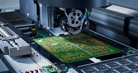
One of the most notable innovations in automated board assembly is the development of surface mount technology (SMT).
SMT has revolutionized the way electronic components are mounted onto printed circuit boards (PCBs). By allowing components to be placed directly onto the surface of the board, SMT eliminates the need for drilling holes, thus streamlining the assembly process. This technique not only reduces manufacturing time but also enables the production of smaller, more compact devices. Furthermore, SMT facilitates higher component density, which is essential for modern electronics that demand increased functionality within limited space.
In addition to SMT, the advent of advanced robotics has significantly impacted automated board assembly.
Robotic systems equipped with sophisticated vision and sensing technologies are now capable of performing intricate tasks with remarkable accuracy. These systems can handle delicate components, ensuring precise placement and alignment, which is crucial for maintaining the integrity of the assembly. Moreover, robotics in board assembly enhances flexibility, allowing manufacturers to quickly adapt to design changes and varying production volumes without compromising efficiency.
Another key innovation is the implementation of machine learning algorithms in automated board assembly processes.
Machine learning enables systems to analyze vast amounts of data generated during assembly, identifying patterns and anomalies that may indicate potential defects. By leveraging this data, manufacturers can optimize assembly parameters in real-time, reducing the likelihood of errors and improving yield rates. This predictive capability not only enhances quality control but also minimizes waste, contributing to more sustainable manufacturing practices.
Furthermore, the integration of the Internet of Things (IoT) in board assembly has opened new avenues for innovation.
IoT-enabled devices can communicate with assembly systems, providing real-time feedback and diagnostics. This connectivity allows for continuous monitoring and optimization of the assembly process, ensuring that any issues are promptly addressed. Additionally, IoT facilitates remote management and control, enabling manufacturers to oversee operations from anywhere in the world, thus enhancing operational efficiency and reducing downtime.
As these innovations continue to shape the landscape of board assembly, it is essential to consider the implications for the workforce.
While automation undoubtedly increases efficiency and reduces costs, it also necessitates a shift in skill requirements. Workers must now possess a deeper understanding of automated systems and data analysis to effectively manage and maintain these advanced technologies. Consequently, ongoing training and education are crucial to ensure that the workforce remains equipped to meet the demands of this rapidly evolving industry.
In conclusion, the innovations in automated board assembly techniques are transforming the manufacturing landscape, offering unprecedented levels of precision, efficiency, and adaptability. As technology continues to advance, it is imperative for manufacturers to embrace these innovations to remain competitive in an increasingly demanding market. By leveraging the capabilities of SMT, robotics, machine learning, and IoT, the industry can achieve new heights in quality and performance, ultimately driving the next generation of electronic devices.
The Importance Of Quality Control In PCB Assembly
In the realm of electronics manufacturing, the assembly of printed circuit boards (PCBs) stands as a critical process that demands precision and attention to detail. As the backbone of electronic devices, PCBs facilitate the connection and communication between various components, ensuring the device functions as intended. Consequently, the importance of quality control in PCB assembly cannot be overstated, as it plays a pivotal role in determining the reliability and performance of the final product.
To begin with, quality control in PCB assembly involves a series of systematic procedures designed to ensure that each board meets specific standards and specifications.
This process begins with the inspection of raw materials, such as the substrate and copper layers, to verify their compliance with industry standards. By ensuring that only high-quality materials are used, manufacturers can prevent defects that may arise from substandard components. Furthermore, this initial step sets the stage for a successful assembly process, as it minimizes the risk of errors that could compromise the integrity of the final product.
As the assembly process progresses, quality control measures continue to play a crucial role.
During the soldering phase, for instance, it is essential to ensure that each component is accurately placed and securely attached to the board. Automated optical inspection (AOI) systems are often employed at this stage to detect any misalignments or soldering defects, such as bridges or insufficient solder joints. By identifying these issues early on, manufacturers can address them promptly, thereby reducing the likelihood of costly rework or product recalls.
Moreover, quality control extends beyond the physical assembly of the board to encompass electrical testing.
Functional testing, in particular, is vital to verify that the assembled PCB operates as intended. This involves subjecting the board to various electrical tests to ensure that all circuits are functioning correctly and that there are no short circuits or open connections. By conducting thorough electrical testing, manufacturers can guarantee that the final product will perform reliably in real-world applications.
In addition to these technical aspects, quality control in PCB assembly also involves adherence to industry standards and regulations.
Compliance with standards such as IPC-A-610, which outlines the acceptability of electronic assemblies, is crucial for ensuring that the assembled boards meet the necessary quality benchmarks. Furthermore, adherence to environmental regulations, such as the Restriction of Hazardous Substances (RoHS) directive, is essential for minimizing the environmental impact of electronic manufacturing.
The implementation of robust quality control measures in PCB assembly not only enhances the reliability and performance of electronic devices but also contributes to the overall efficiency of the manufacturing process. By identifying and addressing potential issues early on, manufacturers can reduce waste, lower production costs, and improve customer satisfaction. Moreover, a strong commitment to quality control can enhance a company’s reputation, as it demonstrates a dedication to delivering high-quality products that meet or exceed customer expectations.
In conclusion, quality control is an indispensable component of PCB assembly, serving as a safeguard against defects and ensuring the reliability of electronic devices. Through meticulous inspection, testing, and adherence to industry standards, manufacturers can produce PCBs that are not only functional but also durable and dependable. As the demand for advanced electronic devices continues to grow, the importance of quality control in PCB assembly will remain paramount, underscoring its role in shaping the future of electronics manufacturing.

Challenges And Solutions In High-Density Board Assembly
In the rapidly evolving world of electronics, high-density board assembly presents a unique set of challenges that manufacturers must navigate to ensure the production of reliable and efficient devices. As consumer demand for smaller, more powerful gadgets continues to grow, the need for compact and densely packed printed circuit boards (PCBs) has become increasingly critical. However, this trend towards miniaturization introduces several complexities in the assembly process, necessitating innovative solutions to overcome these hurdles.
One of the primary challenges in high-density board assembly is the precise placement of components.
As the size of electronic devices decreases, the components themselves become smaller and more numerous, requiring exceptional accuracy during placement. This is compounded by the fact that high-density boards often incorporate a mix of surface-mount technology (SMT) and through-hole components, each with distinct placement requirements. To address this, manufacturers are turning to advanced automated assembly equipment that utilizes sophisticated vision systems and robotics to achieve the necessary precision. These systems are capable of handling the minute tolerances required for high-density assemblies, thereby reducing the risk of misalignment and ensuring optimal performance.
In addition to placement challenges, soldering in high-density board assembly presents its own set of difficulties.
The close proximity of components increases the risk of solder bridging, where excess solder creates unintended connections between adjacent pads or traces. This can lead to short circuits and device failure. To mitigate this risk, manufacturers are employing techniques such as controlled solder paste deposition and reflow soldering profiles tailored to the specific thermal characteristics of the board. Moreover, the use of advanced soldering materials, such as low-residue fluxes and lead-free solders, helps to minimize defects and improve the overall reliability of the assembly.
Another significant challenge is thermal management.
High-density boards often house components that generate substantial heat, which can adversely affect performance and longevity if not properly managed. The limited space on these boards makes it difficult to incorporate traditional cooling solutions, such as heat sinks or fans. Consequently, manufacturers are exploring alternative methods, such as the use of thermal vias and conductive materials within the PCB itself, to dissipate heat more effectively. Additionally, the strategic placement of components and the use of thermal simulation software during the design phase can help identify potential hotspots and optimize the thermal performance of the board.
Signal integrity is also a critical concern in high-density board assembly.
As the number of components and interconnections increases, so does the potential for electromagnetic interference (EMI) and crosstalk, which can degrade signal quality. To combat this, manufacturers are implementing design strategies such as controlled impedance routing and the use of ground planes to shield sensitive signals. Furthermore, the adoption of high-speed digital design techniques and the integration of signal integrity analysis tools into the design process enable engineers to predict and mitigate potential issues before they arise.
In conclusion, while high-density board assembly presents a myriad of challenges, the industry is continually developing innovative solutions to address these complexities. Through the use of advanced automation, precise soldering techniques, effective thermal management, and robust signal integrity strategies, manufacturers are able to produce high-density PCBs that meet the demands of modern electronic devices. As technology continues to advance, the ongoing refinement of these solutions will be essential to maintaining the pace of innovation and ensuring the reliability of next-generation electronics.
Environmental Impact Of Modern Board Assembly Practices
The environmental impact of modern board assembly practices has become an increasingly important topic as the electronics industry continues to expand. With the proliferation of electronic devices, the demand for printed circuit boards (PCBs) has surged, leading to a corresponding increase in the environmental footprint of their production. Understanding the implications of these practices is crucial for developing more sustainable methods and mitigating the adverse effects on our planet.
To begin with, the production of PCBs involves several stages, each contributing to environmental degradation.
The initial phase, which includes the extraction and processing of raw materials, is particularly resource-intensive. Metals such as copper, gold, and tin are essential components of PCBs, and their extraction often results in significant ecological disruption. Mining activities can lead to deforestation, soil erosion, and contamination of water sources, thereby affecting local ecosystems and communities.
Moreover, the manufacturing process itself is energy-intensive and generates substantial waste.
The etching and plating processes used to create the intricate patterns on PCBs require large amounts of water and chemicals, which can result in hazardous waste if not properly managed. The disposal of these chemicals poses a significant risk to the environment, as they can leach into soil and water, causing pollution and harm to aquatic life. Additionally, the energy consumption associated with board assembly contributes to greenhouse gas emissions, further exacerbating climate change.
In recent years, however, there has been a growing awareness of these environmental challenges, prompting the industry to explore more sustainable practices.
One such approach is the adoption of lead-free soldering techniques. Traditional soldering methods often use lead, a toxic metal that poses health risks to workers and environmental hazards when disposed of improperly. By transitioning to lead-free alternatives, manufacturers can reduce the toxicity of their products and minimize their environmental impact.
Furthermore, advancements in technology have enabled the development of more efficient manufacturing processes.
For instance, the use of computer-aided design (CAD) software allows for more precise and optimized board layouts, reducing material waste. Additionally, innovations in recycling and waste management have made it possible to recover valuable materials from discarded electronics, thereby reducing the need for virgin resources and decreasing the overall environmental footprint.
Another promising development is the shift towards using biodegradable materials in board assembly.
Researchers are exploring the use of organic substrates and conductive inks made from renewable resources, which can significantly reduce the environmental impact of PCBs. These materials not only offer a sustainable alternative to traditional components but also facilitate easier recycling and disposal at the end of a product’s life cycle.
Despite these advancements, challenges remain in fully implementing sustainable practices across the industry.
Economic factors, such as the cost of transitioning to new materials and technologies, can be a barrier for some manufacturers. Additionally, the global nature of the electronics supply chain complicates efforts to standardize and enforce environmentally friendly practices.
In conclusion, while modern board assembly practices have historically posed significant environmental challenges, there is a clear shift towards more sustainable methods. By embracing innovations in materials, processes, and recycling, the industry can reduce its ecological footprint and contribute to a more sustainable future. Continued collaboration among manufacturers, policymakers, and researchers will be essential in overcoming the remaining obstacles and ensuring that the environmental impact of board assembly is minimized for generations to come.


